Home > Press > Experimental nanosheet material marks a step toward the next generation of low-power, high-performance electronics
 |
Abstract:
A team of researchers in China have developed a high-conductivity material that could greatly reduce contact resistance and Schottky barrier height within critical parts of electronic and optoelectronic microchips, paving the way for computer and digital imaging components that consume less power relative to their performance than existing chipsets. The material, molybdenum disulfide (MoS2) is so thin that it falls into a classification of two-dimensional. That is, it is grown in sheets extending in two directions, X and Y, but virtually immeasurable on a Z axis because the material is often only a single molecule or atom in height.
Experimental nanosheet material marks a step toward the next generation of low-power, high-performance electronics
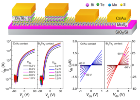
Tsinghua, China | Posted on December 9th, 2022In the article, �Epitaxial van der Waals Contacts for Low Schottky Barrier MoS2 Field Effect Transistors,� the authors emphasize how 2D materials have attracted tremendous attention due to their abundant and tunable electronic states and diverse optical, electronic, and mechanical properties, which make them promising building blocks for future high-performance electronic and optoelectronic devices, such as transistors, photodetectors, and light-emitting diodes. The experiment was an effort to address �The performance of a 2D semiconductor transistor mainly relies on the microscopic connections among components within a chip, and the quality of those connections depends ultimately on the material used in these contact points, which are always metals achieved by thermal evaporation, limiting the performance of 2D materials-based transistors," Li said.
In an effort to develop a higher-performing contact point, Li�s team employed Bismuth Telluride (Bi2Te3), a highly conductivemetalloid and semimetal in combination with semi-conducting MoS2. Growing these metalloid nanosheet crystals together as a hybrid yielded initially promising results.
�Attempts in recent years to achieve epitaxially grown semiconductor contacts have succeeded in laboratory settings, but weren�t likely candidates for being scaled up to the level that would be needed to manufacture chips and other devices,� Li said. �Most of these methods put forward strict requirements for material preparation and strict fabrication and are hardly compatible with further manufacturing processes in integrated circuits. The realization of high-quality semiconducting 2D materials and excellent contact at the same time is critical for reliable device applications.�
The process of fabricating this experimental van der Waals contact involved vertically stacking MoS2 and Bi2Te3 in a two-step synthesis process. As the growth of MoS2 monolayer, molybdenum trioxide (MoO3) powder and sulfur powder were placed at the center and upper stream of the furnace, respectively, and a piece of Silicon dioxide (SiO2) substrate was placed downstream of a quartz tube. For the second step growth of the Bi2Te3 nanosheet, the Bi2Te3 powder and the as-grown MoS2 nanosheets were placed at the center and downstream of the quartz tube, respectively. After 5 minutes of growth, MoS2/Bi2Te3 heterostructures were obtained.. The researchers observed that the growth temperature and gas flow rate during the growth process could influence the thickness and nucleation sites of the Bi2Te3 nanosheets.
The team used a variety of electrical and imaging techniques to observe the appearance and conductive performance of the hybrid nanosheets and found that the new contact method greatly outperformed gold contacts, which are useful as a baseline measurement because of how common gold is in chip manufacturing. The new contact method was tested at different ambient temperatures and maintained good performance at room temperature � a key milestone in making MoS2/Bi2Te3 semiconducting contact method a good candidate for future commercial viability.
�Combining the multiple advantages, the epitaxial van der Waals Bi2Te3 contacts provide a new strategy for the application of 2D MoS2 in future optoelectronic devices,� Li said. �Now that we�ve established the functionality of Bi2Te3 contacts in a controlled laboratory setting, the next steps will be to continue to investigate and optimize this method, with the hope that this new technology can eventually be adopted for widespread use in more powerful, lower energy consumption electronics.�
####
About Tsinghua University Press
Established in 1980, belonging to Tsinghua University, Tsinghua University Press (TUP) is a leading comprehensive higher education and professional publisher in China. Committed to building a top-level global cultural brand, after 41 years of development, TUP has established an outstanding managerial system and enterprise structure, and delivered multimedia and multi-dimensional publications covering books, audio, video, electronic products, journals and digital publications. In addition, TUP actively carries out its strategic transformation from educational publishing to content development and service for teaching & learning and was named First-class National Publisher for achieving remarkable results.
About Nano Research
Nano Research is a peer-reviewed, international and interdisciplinary research journal, publishes all aspects of nano science and technology, featured in rapid review and fast publishing, sponsored by Tsinghua University and the Chinese Chemical Society. It offers readers an attractive mix of authoritative and comprehensive reviews and original cutting-edge research papers. After 15 years of development, it has become one of the most influential academic journals in the nano field. In 2022 InCites Journal Citation Reports, Nano Research has an Impact Factor of 10.269 (9.136, 5 years), the total cites reached 29620, ranking first in China's international academic journals, and the number of highly cited papers reached 120, ranked among the top 2.8% of over 9000 academic journals.
For more information, please click here
Contacts:
Yao Meng
Tsinghua University Press
Office: 86-108-347-0574
Copyright © Tsinghua University Press
If you have a comment, please Contact us.Issuers of news releases, not 7th Wave, Inc. or Nanotechnology Now, are solely responsible for the accuracy of the content.
Bookmark:


| Related Links |
| Related News Press |
News and information
![]() Quantum computer improves AI predictions April 17th, 2026
Quantum computer improves AI predictions April 17th, 2026
![]() Flexible sensor gains sensitivity under pressure April 17th, 2026
Flexible sensor gains sensitivity under pressure April 17th, 2026
![]() A reusable chip for particulate matter sensing April 17th, 2026
A reusable chip for particulate matter sensing April 17th, 2026
![]() Detecting vibrational quantum beating in the predissociation dynamics of SF6 using time-resolved photoelectron spectroscopy April 17th, 2026
Detecting vibrational quantum beating in the predissociation dynamics of SF6 using time-resolved photoelectron spectroscopy April 17th, 2026
2 Dimensional Materials
![]() Flexible sensor gains sensitivity under pressure April 17th, 2026
Flexible sensor gains sensitivity under pressure April 17th, 2026
Govt.-Legislation/Regulation/Funding/Policy
![]() Quantum computer improves AI predictions April 17th, 2026
Quantum computer improves AI predictions April 17th, 2026
![]() Metasurfaces smooth light to boost magnetic sensing precision January 30th, 2026
Metasurfaces smooth light to boost magnetic sensing precision January 30th, 2026
![]() New imaging approach transforms study of bacterial biofilms August 8th, 2025
New imaging approach transforms study of bacterial biofilms August 8th, 2025
Possible Futures
![]() A fundamentally new therapeutic approach to cystic fibrosis: Nanobody repairs cellular defect April 17th, 2026
A fundamentally new therapeutic approach to cystic fibrosis: Nanobody repairs cellular defect April 17th, 2026
![]() UC Irvine physicists discover method to reverse �quantum scrambling� : The work addresses the problem of information loss in quantum computing system April 17th, 2026
UC Irvine physicists discover method to reverse �quantum scrambling� : The work addresses the problem of information loss in quantum computing system April 17th, 2026
Chip Technology
![]() A reusable chip for particulate matter sensing April 17th, 2026
A reusable chip for particulate matter sensing April 17th, 2026
![]() Metasurfaces smooth light to boost magnetic sensing precision January 30th, 2026
Metasurfaces smooth light to boost magnetic sensing precision January 30th, 2026
Optical computing/Photonic computing
![]() ICFO researchers overcome long-standing bottleneck in single photon detection with twisted 2D materials August 8th, 2025
ICFO researchers overcome long-standing bottleneck in single photon detection with twisted 2D materials August 8th, 2025
![]() Programmable electron-induced color router array May 14th, 2025
Programmable electron-induced color router array May 14th, 2025
Discoveries
![]() Quantum computer improves AI predictions April 17th, 2026
Quantum computer improves AI predictions April 17th, 2026
![]() Flexible sensor gains sensitivity under pressure April 17th, 2026
Flexible sensor gains sensitivity under pressure April 17th, 2026
![]() A reusable chip for particulate matter sensing April 17th, 2026
A reusable chip for particulate matter sensing April 17th, 2026
![]() Detecting vibrational quantum beating in the predissociation dynamics of SF6 using time-resolved photoelectron spectroscopy April 17th, 2026
Detecting vibrational quantum beating in the predissociation dynamics of SF6 using time-resolved photoelectron spectroscopy April 17th, 2026
Announcements
![]() A fundamentally new therapeutic approach to cystic fibrosis: Nanobody repairs cellular defect April 17th, 2026
A fundamentally new therapeutic approach to cystic fibrosis: Nanobody repairs cellular defect April 17th, 2026
![]() UC Irvine physicists discover method to reverse �quantum scrambling� : The work addresses the problem of information loss in quantum computing system April 17th, 2026
UC Irvine physicists discover method to reverse �quantum scrambling� : The work addresses the problem of information loss in quantum computing system April 17th, 2026
Interviews/Book Reviews/Essays/Reports/Podcasts/Journals/White papers/Posters
![]() A fundamentally new therapeutic approach to cystic fibrosis: Nanobody repairs cellular defect April 17th, 2026
A fundamentally new therapeutic approach to cystic fibrosis: Nanobody repairs cellular defect April 17th, 2026
![]() UC Irvine physicists discover method to reverse �quantum scrambling� : The work addresses the problem of information loss in quantum computing system April 17th, 2026
UC Irvine physicists discover method to reverse �quantum scrambling� : The work addresses the problem of information loss in quantum computing system April 17th, 2026
Photonics/Optics/Lasers
![]() Metasurfaces smooth light to boost magnetic sensing precision January 30th, 2026
Metasurfaces smooth light to boost magnetic sensing precision January 30th, 2026
![]() From sensors to smart systems: the rise of AI-driven photonic noses January 30th, 2026
From sensors to smart systems: the rise of AI-driven photonic noses January 30th, 2026
|
|
||
|
|
||
| The latest news from around the world, FREE | ||
|
|
||
|
|
||
| Premium Products | ||
|
|
||
|
Only the news you want to read!
Learn More |
||
|
|
||
|
Full-service, expert consulting
Learn More |
||
|
|
||