Home > Press > Building with nanoparticles, from the bottom up: Researchers develop a technique for precisely arranging nanoscale particles on a surface, such as a silicon chip, that doesn’t damage the material
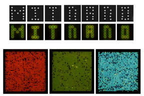 |
| These images show nanoparticles (colored dots) that have been precisely arranged onto different surfaces, using the technique developed by Niroui and her collaborators. Their method is so precise that particles can be arranged into arbitrary shapes, like individual letters that spell "MIT NANO," and then transferred to surfaces with high position accuracy, as seen here. Credits:Image: Courtesy of the researchers |
Abstract:
Researchers at MIT have developed a technique for precisely controlling the arrangement and placement of nanoparticles on a material, like the silicon used for computer chips, in a way that does not damage or contaminate the surface of the material.
Building with nanoparticles, from the bottom up: Researchers develop a technique for precisely arranging nanoscale particles on a surface, such as a silicon chip, that doesn’t damage the material
Cambridge, MA | Posted on October 28th, 2022The technique, which combines chemistry and directed assembly processes with conventional fabrication techniques, enables the efficient formation of high-resolution, nanoscale features integrated with nanoparticles for devices like sensors, lasers, and LEDs, which could boost their performance.
Transistors and other nanoscale devices are typically fabricated from the top down — materials are etched away to reach the desired arrangement of nanostructures. But creating the smallest nanostructures, which can enable the highest performance and new functionalities, requires expensive equipment and remains difficult to do at scale and with the desired resolution.
A more precise way to assemble nanoscale devices is from the bottom up. In one scheme, engineers have used chemistry to “grow” nanoparticles in solution, drop that solution onto a template, arrange the nanoparticles, and then transfer them to a surface. However, this technique also involves steep challenges. First, thousands of nanoparticles must be arranged on the template efficiently. And transferring them to a surface typically requires a chemical glue, large pressure, or high temperatures, which could damage the surfaces and the resulting device.
The MIT researchers developed a new approach to overcome these limitations. They used the powerful forces that exist at the nanoscale to efficiently arrange particles in a desired pattern and then transfer them to a surface without any chemicals or high pressures, and at lower temperatures. Because the surface material remains pristine, these nanoscale structures can be incorporated into components for electronic and optical devices, where even minuscule imperfections can hamper performance.
“This approach allows you, through engineering of forces, to place the nanoparticles, despite their very small size, in deterministic arrangements with single-particle resolution and on diverse surfaces, to create libraries of nanoscale building blocks that can have very unique properties, whether it is their light-matter interactions, electronic properties, mechanical performance, etc.,” says Farnaz Niroui, the EE Landsman Career Development Assistant Professor of Electrical Engineering and Computer Science (EECS) at MIT, a member of the MIT Research Laboratory of Electronics, and senior author on a new paper describing the work. “By integrating these building blocks with other nanostructures and materials we can then achieve devices with unique functionalities that would not be readily feasible to make if we were to use the conventional top-down fabrication strategies alone.”
The research is published in Science Advances. Niroui’s co-authors are lead author Weikun “Spencer” Zhu, a graduate student in the Department of Chemical Engineering, as well as EECS graduate students Peter F. Satterthwaite, Patricia Jastrzebska-Perfect, and Roberto Brenes.
Use the forces
To begin their fabrication method, known as nanoparticle contact printing, the researchers use chemistry to create nanoparticles with a defined size and shape in a solution. To the naked eye, this looks like a vial of colored liquid, but zooming in with an electron microscope would reveal millions of cubes, each just 50 nanometers in size. (A human hair is about 80,000 nanometers wide.)
The researchers then make a template in the form of a flexible surface covered with nanoparticle-sized guides, or traps, that are arranged in the shape they want the nanoparticles to take. After adding a drop of nanoparticle solution to the template, they use two nanoscale forces to move the particles into the right position. The nanoparticles are then transferred onto arbitrary surfaces.
At the nanoscale, different forces become dominant (just like gravity is a dominant force at the macroscale). Capillary forces are dominant when the nanoparticles are in liquid and van der Waals forces are dominant at the interface between the nanoparticles and the solid surface they are in contact with. When the researchers add a drop of liquid and drag it across the template, capillary forces move the nanoparticles into the desired trap, placing them precisely in the right spot. Once the liquid dries, van der Waals forces hold those nanoparticles in position.
“These forces are ubiquitous and can often be detrimental when it comes to the fabrication of nanoscale objects as they can cause the collapse of the structures. But we are able to come up with ways to control these forces very precisely to use them to control how things are manipulated at the nanoscale,” says Zhu.
They design the template guides to be the right size and shape, and in the precisely proper arrangement so the forces work together to arrange the particles. The nanoparticles are then printed onto surfaces without a need for any solvents, surface treatments, or high temperatures. This keeps the surfaces pristine and properties intact while allowing yields of more than 95 percent. To promote this transfer, the surface forces need to be engineered so that the van der Waals forces are strong enough to consistently promote particles to release from the template and attach to the receiving surface when placed in contact.
Unique shapes, diverse materials, scalable processing
The team used this technique to arrange nanoparticles into arbitrary shapes, such as letters of the alphabet, and then transferred them to silicon with very high position accuracy. The method also works with nanoparticles that have other shapes, such as spheres, and with diverse material types. And it can transfer nanoparticles effectively onto different surfaces, like gold or even flexible substrates for next-generation electrical and optical structures and devices.
Their approach is also scalable, so it can be extended to be used toward fabrication of real-world devices.
Niroui and her colleagues are now working to leverage this approach to create even more complex structures and integrate it with other nanoscale materials to develop new types of electronic and optical devices.
This work was supported, in part, by the National Science Foundation (NSF) and the NSF Graduate Research Fellowship Program.
###
Written by Adam Zewe, MIT News Office
####
For more information, please click here
Contacts:
Abby Abazorius
Massachusetts Institute of Technology
Office: 617-253-2709
Copyright © Massachusetts Institute of Technology
If you have a comment, please Contact us.Issuers of news releases, not 7th Wave, Inc. or Nanotechnology Now, are solely responsible for the accuracy of the content.
Bookmark:


| Related Links |
| Related News Press |
News and information
![]() Quantum computer improves AI predictions April 17th, 2026
Quantum computer improves AI predictions April 17th, 2026
![]() Flexible sensor gains sensitivity under pressure April 17th, 2026
Flexible sensor gains sensitivity under pressure April 17th, 2026
![]() A reusable chip for particulate matter sensing April 17th, 2026
A reusable chip for particulate matter sensing April 17th, 2026
![]() Detecting vibrational quantum beating in the predissociation dynamics of SF6 using time-resolved photoelectron spectroscopy April 17th, 2026
Detecting vibrational quantum beating in the predissociation dynamics of SF6 using time-resolved photoelectron spectroscopy April 17th, 2026
Possible Futures
![]() A fundamentally new therapeutic approach to cystic fibrosis: Nanobody repairs cellular defect April 17th, 2026
A fundamentally new therapeutic approach to cystic fibrosis: Nanobody repairs cellular defect April 17th, 2026
![]() UC Irvine physicists discover method to reverse ‘quantum scrambling’ : The work addresses the problem of information loss in quantum computing system April 17th, 2026
UC Irvine physicists discover method to reverse ‘quantum scrambling’ : The work addresses the problem of information loss in quantum computing system April 17th, 2026
Chip Technology
![]() A reusable chip for particulate matter sensing April 17th, 2026
A reusable chip for particulate matter sensing April 17th, 2026
![]() Metasurfaces smooth light to boost magnetic sensing precision January 30th, 2026
Metasurfaces smooth light to boost magnetic sensing precision January 30th, 2026
Optical computing/Photonic computing
![]() ICFO researchers overcome long-standing bottleneck in single photon detection with twisted 2D materials August 8th, 2025
ICFO researchers overcome long-standing bottleneck in single photon detection with twisted 2D materials August 8th, 2025
![]() Programmable electron-induced color router array May 14th, 2025
Programmable electron-induced color router array May 14th, 2025
Discoveries
![]() Quantum computer improves AI predictions April 17th, 2026
Quantum computer improves AI predictions April 17th, 2026
![]() Flexible sensor gains sensitivity under pressure April 17th, 2026
Flexible sensor gains sensitivity under pressure April 17th, 2026
![]() A reusable chip for particulate matter sensing April 17th, 2026
A reusable chip for particulate matter sensing April 17th, 2026
![]() Detecting vibrational quantum beating in the predissociation dynamics of SF6 using time-resolved photoelectron spectroscopy April 17th, 2026
Detecting vibrational quantum beating in the predissociation dynamics of SF6 using time-resolved photoelectron spectroscopy April 17th, 2026
Announcements
![]() A fundamentally new therapeutic approach to cystic fibrosis: Nanobody repairs cellular defect April 17th, 2026
A fundamentally new therapeutic approach to cystic fibrosis: Nanobody repairs cellular defect April 17th, 2026
![]() UC Irvine physicists discover method to reverse ‘quantum scrambling’ : The work addresses the problem of information loss in quantum computing system April 17th, 2026
UC Irvine physicists discover method to reverse ‘quantum scrambling’ : The work addresses the problem of information loss in quantum computing system April 17th, 2026
Interviews/Book Reviews/Essays/Reports/Podcasts/Journals/White papers/Posters
![]() A fundamentally new therapeutic approach to cystic fibrosis: Nanobody repairs cellular defect April 17th, 2026
A fundamentally new therapeutic approach to cystic fibrosis: Nanobody repairs cellular defect April 17th, 2026
![]() UC Irvine physicists discover method to reverse ‘quantum scrambling’ : The work addresses the problem of information loss in quantum computing system April 17th, 2026
UC Irvine physicists discover method to reverse ‘quantum scrambling’ : The work addresses the problem of information loss in quantum computing system April 17th, 2026
Photonics/Optics/Lasers
![]() Metasurfaces smooth light to boost magnetic sensing precision January 30th, 2026
Metasurfaces smooth light to boost magnetic sensing precision January 30th, 2026
![]() From sensors to smart systems: the rise of AI-driven photonic noses January 30th, 2026
From sensors to smart systems: the rise of AI-driven photonic noses January 30th, 2026
|
|
||
|
|
||
| The latest news from around the world, FREE | ||
|
|
||
|
|
||
| Premium Products | ||
|
|
||
|
Only the news you want to read!
Learn More |
||
|
|
||
|
Full-service, expert consulting
Learn More |
||
|
|
||