Home > Press > Boron nitride with a twist could lead to new way to make qubits: Easy control over bright emissions from the crystalline material offer a route toward scalable quantum computing and sensing
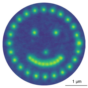 |
| An electron beam placed at a series of locations on a sheet of twisted hBN intensifies the light emission from each location. The brightness depends on how long the beam sits at a given point, or the electron flux delivered to that point. The result is an illuminated pattern. CREDIT Su et al. 2022 |
Abstract:
Achieving scalability in quantum processors, sensors, and networks requires novel devices that are easily manipulated between two quantum states. A team led by researchers from the Department of Energy’s Lawrence Berkeley National Laboratory (Berkeley Lab) has now developed a method, using a solid-state “twisted” crystalline layered material, which gives rise to tiny light-emitting points called color centers. These color centers can be switched on and off with the simple application of an external voltage.
Boron nitride with a twist could lead to new way to make qubits: Easy control over bright emissions from the crystalline material offer a route toward scalable quantum computing and sensing
Berkeley, CA | Posted on October 7th, 2022“This is a first step toward a color center device that engineers could build or adapt into real quantum systems,” said Shaul Aloni, a staff scientist at Berkeley Lab’s Molecular Foundry, who co-led the study. The work is detailed in the journal Nature Materials.
For example, the research could lead to a new way to make quantum bits, or qubits, which encode information in quantum computers.
Color centers are microscopic defects in a crystal, such as diamond, that usually emit bright and stable light of specific color when struck with laser or other energy source such as an electron beam. Their integration with waveguides, devices that guide light, can connect operations across a quantum processor. Several years ago researchers discovered that color centers in a synthesized material called hexagonal boron nitride (hBN), which is commonly used as a lubricant or additive for paints and cosmetics, emitted even brighter colors than color centers in diamond. But engineers have struggled to use the material in applications because producing the defects at a determined location is difficult, and they lacked a reliable way to switch the color centers on and off.
The Berkeley Lab team now solves these problems. Cong Su, a postdoc from the research group led by Alex Zettl, a faculty senior scientist at Berkeley Lab and professor of physics at UC Berkeley, examined how color centers behaved in different sophisticated forms of hBN. The researchers found that two stacked and twisted layers of the material resulted in the activation and enhancement of ultraviolet (UV) emission from a color center, which can be shut off when a voltage is applied across the structure. “It’s like a sandwich with two pieces of bread, but one rotated relative to the other,” said Zettl. The rotation between the two layers activates the color centers at the interface to become extremely bright. The applied voltage then easily and reversibly tunes the intensity from bright to completely dark, without “unrotating” the halves.
Aloni’s development of a modified electron microscope that not only probed the material’s structure but also collected the emitted light for analysis turned out to be key for this study. The setup uses an electron beam to excite the color centers; the researchers also found that they could use the electron beam to activate color centers and draw patterns, such as a smiley face, onto hBN. “People typically zap the material with lasers or ions, but we’ve instead zapped it with a beam of electrons,” said Zettl.
The study achieves three steps toward realization of a scalable quantum device. First, the UV color centers in hBN can be reliably activated to exceptional maximum brightness, by twisting the crystal interface. Second, these color centers can then be gradually and reversibly dimmed by a simple applied voltage. Finally, electron beam treatment allows further precise spatial positioning of these color centers.
Theoretical calculations led by Steven Louie, a faculty senior scientist at Berkeley Lab and distinguished professor of physics at UC Berkeley, provided candidates for the UV color center atomic configuration to help explain why their brightness depended on the twist angle. The light emission process involves an excited electron wandering around and recombining with a hole at the color center. But a typical hBN structure has many traps that could capture the electrons, preventing light emission. “Twisting the crystal layers removes many of these traps, or ‘quantum parking lots,’ near the interface,” said Louie.
The team next intends to prepare samples that allow atomic characterization to pinpoint the specific atomic structures behind this mechanism and add additional levels of control. “The work is pointing us in the direction of new types of mechanisms that we can use to control the emission even better, and this is very important for many applications in quantum information sciences,” said Aloni.
The Molecular Foundry is an Office of Science user facility at Berkeley Lab.
This work was supported by the DOE Office of Science.
####
About DOE/Lawrence Berkeley National Laboratory
Founded in 1931 on the belief that the biggest scientific challenges are best addressed by teams, Lawrence Berkeley National Laboratory and its scientists have been recognized with 14 Nobel Prizes. Today, Berkeley Lab researchers develop sustainable energy and environmental solutions, create useful new materials, advance the frontiers of computing, and probe the mysteries of life, matter, and the universe. Scientists from around the world rely on the Lab’s facilities for their own discovery science. Berkeley Lab is a multiprogram national laboratory, managed by the University of California for the U.S. Department of Energy’s Office of Science.
DOE’s Office of Science is the single largest supporter of basic research in the physical sciences in the United States, and is working to address some of the most pressing challenges of our time. For more information, please visit energy.gov/science.
For more information, please click here
Contacts:
Media Relations
DOE/Lawrence Berkeley National Laboratory
Copyright © DOE/Lawrence Berkeley National Laboratory
If you have a comment, please Contact us.Issuers of news releases, not 7th Wave, Inc. or Nanotechnology Now, are solely responsible for the accuracy of the content.
Bookmark:


| Related Links |
| Related News Press |
News and information
![]() Quantum computer improves AI predictions April 17th, 2026
Quantum computer improves AI predictions April 17th, 2026
![]() Flexible sensor gains sensitivity under pressure April 17th, 2026
Flexible sensor gains sensitivity under pressure April 17th, 2026
![]() A reusable chip for particulate matter sensing April 17th, 2026
A reusable chip for particulate matter sensing April 17th, 2026
![]() Detecting vibrational quantum beating in the predissociation dynamics of SF6 using time-resolved photoelectron spectroscopy April 17th, 2026
Detecting vibrational quantum beating in the predissociation dynamics of SF6 using time-resolved photoelectron spectroscopy April 17th, 2026
Laboratories
![]() Researchers develop molecular qubits that communicate at telecom frequencies October 3rd, 2025
Researchers develop molecular qubits that communicate at telecom frequencies October 3rd, 2025
![]() A battery’s hopping ions remember where they’ve been: Seen in atomic detail, the seemingly smooth flow of ions through a battery’s electrolyte is surprisingly complicated February 16th, 2024
A battery’s hopping ions remember where they’ve been: Seen in atomic detail, the seemingly smooth flow of ions through a battery’s electrolyte is surprisingly complicated February 16th, 2024
Govt.-Legislation/Regulation/Funding/Policy
![]() Quantum computer improves AI predictions April 17th, 2026
Quantum computer improves AI predictions April 17th, 2026
![]() Metasurfaces smooth light to boost magnetic sensing precision January 30th, 2026
Metasurfaces smooth light to boost magnetic sensing precision January 30th, 2026
![]() New imaging approach transforms study of bacterial biofilms August 8th, 2025
New imaging approach transforms study of bacterial biofilms August 8th, 2025
Possible Futures
![]() A fundamentally new therapeutic approach to cystic fibrosis: Nanobody repairs cellular defect April 17th, 2026
A fundamentally new therapeutic approach to cystic fibrosis: Nanobody repairs cellular defect April 17th, 2026
![]() UC Irvine physicists discover method to reverse ‘quantum scrambling’ : The work addresses the problem of information loss in quantum computing system April 17th, 2026
UC Irvine physicists discover method to reverse ‘quantum scrambling’ : The work addresses the problem of information loss in quantum computing system April 17th, 2026
Chip Technology
![]() A reusable chip for particulate matter sensing April 17th, 2026
A reusable chip for particulate matter sensing April 17th, 2026
![]() Metasurfaces smooth light to boost magnetic sensing precision January 30th, 2026
Metasurfaces smooth light to boost magnetic sensing precision January 30th, 2026
Discoveries
![]() Quantum computer improves AI predictions April 17th, 2026
Quantum computer improves AI predictions April 17th, 2026
![]() Flexible sensor gains sensitivity under pressure April 17th, 2026
Flexible sensor gains sensitivity under pressure April 17th, 2026
![]() A reusable chip for particulate matter sensing April 17th, 2026
A reusable chip for particulate matter sensing April 17th, 2026
![]() Detecting vibrational quantum beating in the predissociation dynamics of SF6 using time-resolved photoelectron spectroscopy April 17th, 2026
Detecting vibrational quantum beating in the predissociation dynamics of SF6 using time-resolved photoelectron spectroscopy April 17th, 2026
Announcements
![]() A fundamentally new therapeutic approach to cystic fibrosis: Nanobody repairs cellular defect April 17th, 2026
A fundamentally new therapeutic approach to cystic fibrosis: Nanobody repairs cellular defect April 17th, 2026
![]() UC Irvine physicists discover method to reverse ‘quantum scrambling’ : The work addresses the problem of information loss in quantum computing system April 17th, 2026
UC Irvine physicists discover method to reverse ‘quantum scrambling’ : The work addresses the problem of information loss in quantum computing system April 17th, 2026
Interviews/Book Reviews/Essays/Reports/Podcasts/Journals/White papers/Posters
![]() A fundamentally new therapeutic approach to cystic fibrosis: Nanobody repairs cellular defect April 17th, 2026
A fundamentally new therapeutic approach to cystic fibrosis: Nanobody repairs cellular defect April 17th, 2026
![]() UC Irvine physicists discover method to reverse ‘quantum scrambling’ : The work addresses the problem of information loss in quantum computing system April 17th, 2026
UC Irvine physicists discover method to reverse ‘quantum scrambling’ : The work addresses the problem of information loss in quantum computing system April 17th, 2026
|
|
||
|
|
||
| The latest news from around the world, FREE | ||
|
|
||
|
|
||
| Premium Products | ||
|
|
||
|
Only the news you want to read!
Learn More |
||
|
|
||
|
Full-service, expert consulting
Learn More |
||
|
|
||