Home > Press > ACM Research Launches New Furnace Tool for Thermal Atomic Layer Deposition to Support Advanced Semiconductor Manufacturing Requirements: Ultra Fn A Furnace Tool Shipped to China-Based Foundry Customer
 |
Abstract:
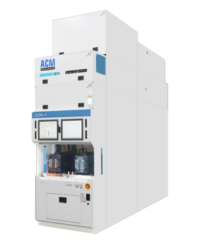
ACM Research, Inc. (ACM) (NASDAQ: ACMR), a leading supplier of wafer processing solutions for semiconductor and advanced wafer-level packaging (WLP) applications, today announced that it has expanded its 300mm Ultra Fn furnace dry processing platform with the introduction of its Ultra Fn A furnace tool. The Ultra Fn A system adds thermal atomic layer deposition (ALD) to ACM’s extensive list of supported furnace applications. The company also announced that it has shipped the first Ultra Fn A furnace tool to a top-tier China-based foundry manufacturer. The product is expected to be qualified in 2023.
ACM Research Launches New Furnace Tool for Thermal Atomic Layer Deposition to Support Advanced Semiconductor Manufacturing Requirements: Ultra Fn A Furnace Tool Shipped to China-Based Foundry Customer
Fremont, CA | Posted on September 30th, 2022“As logic nodes continue to shrink, customers are increasingly looking for suppliers that are willing to collaborate to meet their advanced process requirements, like ALD,” said David Wang, CEO and president of ACM. “ALD is one of the fastest growing applications for manufacturing at advanced nodes, making it a critical new capability for our furnace portfolio. ACM’s deep understanding of the entire semiconductor manufacturing process and our innovative capabilities allow us to quickly develop new applications – wet and dry – to meet emerging market requirements. Our new ALD tool builds on our extensive furnace platform, which also includes support for atmospheric, low-pressure and ultra-high vacuum furnace options.”
About ACM’s Ultra Fn A Furnace Tool
ACM’s new thermal ALD tool deposits both silicon nitride (SiN) and silicon carbide nitride (SiCN) films. The initial Ultra Fn A tool is expected to be used to manufacture the side wall spacer layer in a 28nm logic manufacturing flow, a process which demands a very low etch rate and good step coverage. ACM’s Ultra Fn A furnace tool with proprietary technology has achieved an improvement in uniformity in simulations as compared with competitive approaches.
ACM’s Ultra Fn A tool builds on the success of ACM’s Ultra Fn furnace platform, which meets the dry processing challenges of LPCVD, oxidation, ultra-high vacuum anneal for alloy, high temperature and other common furnace processes. The Ultra Fn A furnace tool was designed from the ground-up to meet best-in-class requirements for high-throughput batch ALD processing. It can be easily customized with minor component and layout changes, which contributed to accelerated development of new types of ALD processes. Its innovative design also combines ACM’s proven software technology with new hardware that improves durability and reliability, as well as ACM’s proprietary process-control IP to provide rapid, stable process control.
Learn more about the Ultra Fn Furnace portfolio and supported applications.
####
About ACM Research, Inc.
ACM develops, manufactures and sells semiconductor process equipment for single-wafer or batch wet cleaning, electroplating, stress-free polishing and thermal processes, which are critical to advanced semiconductor device manufacturing and wafer-level packaging. The company is committed to delivering customized, high-performance, cost-effective process solutions that semiconductor manufacturers can use in numerous manufacturing steps to improve productivity and product yield. For more information, visit www.acmrcsh.com.
© ACM Research, Inc. The ACM Research logo is a trademark of ACM Research, Inc. For convenience, this trademark appears in this press release without a ™ symbol, but that practice does not mean that ACM will not assert, to the fullest extent under applicable law, its rights to such trademark.
For more information, please click here
Contacts:
Media Contact: Company Contacts:
Jillian Carapella USA
Kiterocket Robert Metter
+1 646.402.2408 ACM Research, Inc.
+1 503.367.9753
China
Xi Wang
ACM Research (Shanghai), Inc.
+86 21 50808868
Korea
YY Kim
ACM Research (Korea), Inc.
+821041415171
Taiwan
David Chang
+886 921999884
Singapore
Adrian Ong
+65 8813-1107
Copyright © ACM Research, Inc.
If you have a comment, please Contact us.Issuers of news releases, not 7th Wave, Inc. or Nanotechnology Now, are solely responsible for the accuracy of the content.
Bookmark:


| Related News Press |
News and information
![]() Quantum computer improves AI predictions April 17th, 2026
Quantum computer improves AI predictions April 17th, 2026
![]() Flexible sensor gains sensitivity under pressure April 17th, 2026
Flexible sensor gains sensitivity under pressure April 17th, 2026
![]() A reusable chip for particulate matter sensing April 17th, 2026
A reusable chip for particulate matter sensing April 17th, 2026
![]() Detecting vibrational quantum beating in the predissociation dynamics of SF6 using time-resolved photoelectron spectroscopy April 17th, 2026
Detecting vibrational quantum beating in the predissociation dynamics of SF6 using time-resolved photoelectron spectroscopy April 17th, 2026
Possible Futures
![]() A fundamentally new therapeutic approach to cystic fibrosis: Nanobody repairs cellular defect April 17th, 2026
A fundamentally new therapeutic approach to cystic fibrosis: Nanobody repairs cellular defect April 17th, 2026
![]() UC Irvine physicists discover method to reverse ‘quantum scrambling’ : The work addresses the problem of information loss in quantum computing system April 17th, 2026
UC Irvine physicists discover method to reverse ‘quantum scrambling’ : The work addresses the problem of information loss in quantum computing system April 17th, 2026
Chip Technology
![]() A reusable chip for particulate matter sensing April 17th, 2026
A reusable chip for particulate matter sensing April 17th, 2026
![]() Metasurfaces smooth light to boost magnetic sensing precision January 30th, 2026
Metasurfaces smooth light to boost magnetic sensing precision January 30th, 2026
Announcements
![]() A fundamentally new therapeutic approach to cystic fibrosis: Nanobody repairs cellular defect April 17th, 2026
A fundamentally new therapeutic approach to cystic fibrosis: Nanobody repairs cellular defect April 17th, 2026
![]() UC Irvine physicists discover method to reverse ‘quantum scrambling’ : The work addresses the problem of information loss in quantum computing system April 17th, 2026
UC Irvine physicists discover method to reverse ‘quantum scrambling’ : The work addresses the problem of information loss in quantum computing system April 17th, 2026
Tools
![]() Metasurfaces smooth light to boost magnetic sensing precision January 30th, 2026
Metasurfaces smooth light to boost magnetic sensing precision January 30th, 2026
![]() From sensors to smart systems: the rise of AI-driven photonic noses January 30th, 2026
From sensors to smart systems: the rise of AI-driven photonic noses January 30th, 2026
![]() Japan launches fully domestically produced quantum computer: Expo visitors to experience quantum computing firsthand August 8th, 2025
Japan launches fully domestically produced quantum computer: Expo visitors to experience quantum computing firsthand August 8th, 2025
|
|
||
|
|
||
| The latest news from around the world, FREE | ||
|
|
||
|
|
||
| Premium Products | ||
|
|
||
|
Only the news you want to read!
Learn More |
||
|
|
||
|
Full-service, expert consulting
Learn More |
||
|
|
||