Home > Press > The best semiconductor of them all? Researchers have found a material that can perform much better than silicon. The next step is finding practical and economic ways to make it
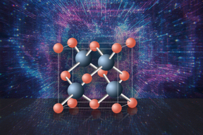 |
| A team of researchers say cubic boron arsenide is the best semiconductor material ever found, and maybe the best possible one. CREDIT Christine Daniloff/MIT |
Abstract:
Silicon is one of the most abundant elements on Earth, and in its pure form the material has become the foundation of much of modern technology, from solar cells to computer chips. But silicon’s properties as a semiconductor are far from ideal.
The best semiconductor of them all? Researchers have found a material that can perform much better than silicon. The next step is finding practical and economic ways to make it
Cambridge, MA | Posted on July 22nd, 2022For one thing, although silicon lets electrons whizz through its structure easily, it is much less accommodating to “holes” — electrons’ positively charged counterparts — and harnessing both is important for some kinds of chips. What’s more, silicon is not very good at conducting heat, which is why overheating issues and expensive cooling systems are common in computers.
Now, a team of researchers at MIT, the University of Houston, and other institutions has carried out experiments showing that a material known as cubic boron arsenide overcomes both of these limitations. It provides high mobility to both electrons and holes, and has excellent thermal conductivity. It is, the researchers say, the best semiconductor material ever found, and maybe the best possible one.
So far, cubic boron arsenide has only been made and tested in small, lab-scale batches that are not uniform. The researchers had to use special methods originally developed by former MIT postdoc Bai Song to test small regions within the material. More work will be needed to determine whether cubic boron arsenide can be made in a practical, economical form, much less replace the ubiquitous silicon. But even in the near future, the material could find some uses where its unique properties would make a significant difference, the researchers say.
The findings are reported in the journal Science, in a paper by MIT postdoc Jungwoo Shin and MIT professor of mechanical engineering Gang Chen; Zhifeng Ren at the University of Houston; and 14 others at MIT, the University of Houston, the University of Texas at Austin, and Boston College.
Earlier research, including work by David Broido, who is a co-author of the new paper, had theoretically predicted that the material would have high thermal conductivity; subsequent work proved that prediction experimentally. This latest work completes the analysis by confirming experimentally a prediction made by Chen’s group back in 2018: that cubic boron arsenide would also have very high mobility for both electrons and holes, “which makes this material really unique,” says Chen.
The earlier experiments showed that the thermal conductivity of cubic boron arsenide is almost 10 times greater than that of silicon. “So, that is very attractive just for heat dissipation,” Chen says. They also showed that the material has a very good bandgap, a property that gives it great potential as a semiconductor material.
Now, the new work fills in the picture, showing that, with its high mobility for both electrons and holes, boron arsenide has all the main qualities needed for an ideal semiconductor. “That’s important because of course in semiconductors we have both positive and negative charges equivalently. So, if you build a device, you want to have a material where both electrons and holes travel with less resistance,” Chen says.
Silicon has good electron mobility but poor hole mobility, and other materials such as gallium arsenide, widely used for lasers, similarly have good mobility for electrons but not for holes.
“Heat is now a major bottleneck for many electronics,” says Shin, the paper’s lead author. “Silicon carbide is replacing silicon for power electronics in major EV industries including Tesla, since it has three times higher thermal conductivity than silicon despite its lower electrical mobilities. Imagine what boron arsenides can achieve, with 10 times higher thermal conductivity and much higher mobility than silicon. It can be a gamechanger.”
Shin adds, “The critical milestone that makes this discovery possible is advances in ultrafast laser grating systems at MIT,” initially developed by Song. Without that technique, he says, it would not have been possible to demonstrate the material’s high mobility for electrons and holes.
The electronic properties of cubic boron arsenide were initially predicted based on quantum mechanical density function calculations made by Chen’s group, he says, and those predictions have now been validated through experiments conducted at MIT, using optical detection methods on samples made by Ren and members of the team at the University of Houston.
Not only is the material’s thermal conductivity the best of any semiconductor, the researchers say, it has the third-best thermal conductivity of any material — next to diamond and isotopically enriched cubic boron nitride. “And now, we predicted the electron and hole quantum mechanical behavior, also from first principles, and that is also proven to be true,” Chen says.
“This is impressive, because I actually don’t know of any other material, other than graphene, that has all these properties,” he says. “And this is a bulk material that has these properties.”
The challenge now, he says, is to figure out practical ways of making this material in usable quantities. The current methods of making it produce very nonuniform material, so the team had to find ways to test just small local patches of the material that were uniform enough to provide reliable data. While they have demonstrated the great potential of this material, “whether or where it’s going to actually be used, we do not know,” Chen says.
“Silicon is the workhorse of the entire industry,” says Chen. “So, OK, we’ve got a material that’s better, but is it actually going to offset the industry? We don’t know.” While the material appears to be almost an ideal semiconductor, “whether it can actually get into a device and replace some of the current market, I think that still has yet to be proven.”
And while the thermal and electrical properties have been shown to be excellent, there are many other properties of a material that have yet to be tested, such as its long-term stability, Chen says. “To make devices, there are many other factors that we don’t know yet.”
He adds, “This potentially could be really important, and people haven’t really even paid attention to this material.” Now that boron arsenide’s desirable properties have become more clear, suggesting the material is “in many ways the best semiconductor,” he says, “maybe there will be more attention paid to this material.”
For commercial uses, Ren says, “one grand challenge would be how to produce and purify cubic boron arsenide as effectively as silicon. … Silicon took decades to win the crown, having purity of over 99.99999999 percent, or ‘10 nines’ for mass production today.”
For it to become practical on the market, Chen says, “it really requires more people to develop different ways to make better materials and characterize them.” Whether the necessary funding for such development will be available remains to be seen, he says.
The research was supported by the U.S. Office of Naval Research, and used facilities of MIT’s MRSEC Shared Experimental Facilities, supported by the National Science Foundation.
###
Written by David L. Chandler, MIT News Office
####
For more information, please click here
Contacts:
Abby Abazorius
Massachusetts Institute of Technology
Office: 617-253-2709
Copyright © Massachusetts Institute of Technology
If you have a comment, please Contact us.Issuers of news releases, not 7th Wave, Inc. or Nanotechnology Now, are solely responsible for the accuracy of the content.
Bookmark:


| Related Links |
| Related News Press |
News and information
![]() Quantum computer improves AI predictions April 17th, 2026
Quantum computer improves AI predictions April 17th, 2026
![]() Flexible sensor gains sensitivity under pressure April 17th, 2026
Flexible sensor gains sensitivity under pressure April 17th, 2026
![]() A reusable chip for particulate matter sensing April 17th, 2026
A reusable chip for particulate matter sensing April 17th, 2026
![]() Detecting vibrational quantum beating in the predissociation dynamics of SF6 using time-resolved photoelectron spectroscopy April 17th, 2026
Detecting vibrational quantum beating in the predissociation dynamics of SF6 using time-resolved photoelectron spectroscopy April 17th, 2026
Possible Futures
![]() A fundamentally new therapeutic approach to cystic fibrosis: Nanobody repairs cellular defect April 17th, 2026
A fundamentally new therapeutic approach to cystic fibrosis: Nanobody repairs cellular defect April 17th, 2026
![]() UC Irvine physicists discover method to reverse ‘quantum scrambling’ : The work addresses the problem of information loss in quantum computing system April 17th, 2026
UC Irvine physicists discover method to reverse ‘quantum scrambling’ : The work addresses the problem of information loss in quantum computing system April 17th, 2026
Chip Technology
![]() A reusable chip for particulate matter sensing April 17th, 2026
A reusable chip for particulate matter sensing April 17th, 2026
![]() Metasurfaces smooth light to boost magnetic sensing precision January 30th, 2026
Metasurfaces smooth light to boost magnetic sensing precision January 30th, 2026
Discoveries
![]() Quantum computer improves AI predictions April 17th, 2026
Quantum computer improves AI predictions April 17th, 2026
![]() Flexible sensor gains sensitivity under pressure April 17th, 2026
Flexible sensor gains sensitivity under pressure April 17th, 2026
![]() A reusable chip for particulate matter sensing April 17th, 2026
A reusable chip for particulate matter sensing April 17th, 2026
![]() Detecting vibrational quantum beating in the predissociation dynamics of SF6 using time-resolved photoelectron spectroscopy April 17th, 2026
Detecting vibrational quantum beating in the predissociation dynamics of SF6 using time-resolved photoelectron spectroscopy April 17th, 2026
Announcements
![]() A fundamentally new therapeutic approach to cystic fibrosis: Nanobody repairs cellular defect April 17th, 2026
A fundamentally new therapeutic approach to cystic fibrosis: Nanobody repairs cellular defect April 17th, 2026
![]() UC Irvine physicists discover method to reverse ‘quantum scrambling’ : The work addresses the problem of information loss in quantum computing system April 17th, 2026
UC Irvine physicists discover method to reverse ‘quantum scrambling’ : The work addresses the problem of information loss in quantum computing system April 17th, 2026
Interviews/Book Reviews/Essays/Reports/Podcasts/Journals/White papers/Posters
![]() A fundamentally new therapeutic approach to cystic fibrosis: Nanobody repairs cellular defect April 17th, 2026
A fundamentally new therapeutic approach to cystic fibrosis: Nanobody repairs cellular defect April 17th, 2026
![]() UC Irvine physicists discover method to reverse ‘quantum scrambling’ : The work addresses the problem of information loss in quantum computing system April 17th, 2026
UC Irvine physicists discover method to reverse ‘quantum scrambling’ : The work addresses the problem of information loss in quantum computing system April 17th, 2026
|
|
||
|
|
||
| The latest news from around the world, FREE | ||
|
|
||
|
|
||
| Premium Products | ||
|
|
||
|
Only the news you want to read!
Learn More |
||
|
|
||
|
Full-service, expert consulting
Learn More |
||
|
|
||