Home > Press > Photon-controlled diode: an optoelectronic device with a new signal processing behavior
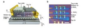 |
| a. Schematic of a photon-controlled diode fabricated by sandwiching a h-BN layer between a n/n− MoS2 junction and a SiO2/p+-Si back-gate, using bottom/top graphene as cathode/anode and a top h-BN as protecting mask. b. Optical photograph of the fabricated array using photon-controlled diode as a unit. (scale bar: 10 μm). CREDIT �Science China Press |
Abstract:
A photodetector is a kind of optoelectronic device that can detect optical signals and convert them into electrical signals, which includes photodiodes, phototransistors and photoconductors, et al. Although there are many types of photodetectors with different mechanisms and structures, depending on their electrical output characteristics before and after illumination, the representative behavior can be summarized as a limited number: the output current of a photodiode changes from rectified to fully-on state after illumination, while the output current of a photoconductor or a phototransistor changes from fully-off to fully-on state. From the perspective of the signal change behavior, there should be a new device that changes the output current from fully-off to rectified state, and may play a key role in future optoelectronic systems, such as optical logic, high-precision imaging and information processing. For instance, rectification controlled by light can avoid the crosstalk issue of photodetector arrays without using selectors, thereby helping to further improve the integration of the array.
Photon-controlled diode: an optoelectronic device with a new signal processing behavior
Beijing, China | Posted on July 1st, 2022Recently, in a paper published in National Science Review, Dong-Ming Sun Group of the Institute of Metal Research, Chinese Academy of Sciences proposes a new device named photon-controlled diode which can change the output current from a fully-off state to a rectified state after illumination for the first time, leading to an anti-crosstalk photomemory array without using any selectors.
Scientists use lateral n/n− molybdenum disulfide (MoS2) junction as a channel, graphene as contact electrodes and hexagonal boron nitride (h-BN) as a photogating layer material to fabricate the photon-controlled diode, which is essentially a n/n− MoS2 junction inserted between two graphene/MoS2 Schottky junctions at the cathode and the anode. Controlled by light, the Schottky junctions suppress or permit the rectification behavior of the n/n− junction, so that the output current of the photon-controlled diode can change from fully-off to rectified state. The light-to-dark rectification ratio can be as high as more than 106. As a photodetector, its responsivity exceeds 105 A/W, while by increasing the thickness of the photogating layer, the behavior of the device changes to a multifunctional photomemory with the highest nonvolatile responsivity of 4.8�107 A/W and the longest retention time of 6.5 � 106 s reported so far. Using the photon-controlled diodes as pixel units, a 3�3 photomemory array is fabricated without using any selectors, showing no crosstalk as well as functions of wavelength and power density selectivity. This work paves the way for the development of future high-integration, low-power and intelligent optoelectronic systems.
This research received funding from the National Natural Science Foundation of China.
####
For more information, please click here
Contacts:
Bei Yan
Science China Press
Office: 86-10-64015905
Expert Contact
Dong-Ming Sun
Shenyang National Laboratory for Materials Science, Institute of Metal Research, Chinese Academy of Sciences.
Copyright © Science China Press
If you have a comment, please Contact us.Issuers of news releases, not 7th Wave, Inc. or Nanotechnology Now, are solely responsible for the accuracy of the content.
Bookmark:


| Related Links |
![]() A photon-controlled diode with a new signal processing behavior:
A photon-controlled diode with a new signal processing behavior:
| Related News Press |
News and information
![]() Quantum computer improves AI predictions April 17th, 2026
Quantum computer improves AI predictions April 17th, 2026
![]() Flexible sensor gains sensitivity under pressure April 17th, 2026
Flexible sensor gains sensitivity under pressure April 17th, 2026
![]() A reusable chip for particulate matter sensing April 17th, 2026
A reusable chip for particulate matter sensing April 17th, 2026
![]() Detecting vibrational quantum beating in the predissociation dynamics of SF6 using time-resolved photoelectron spectroscopy April 17th, 2026
Detecting vibrational quantum beating in the predissociation dynamics of SF6 using time-resolved photoelectron spectroscopy April 17th, 2026
Possible Futures
![]() A fundamentally new therapeutic approach to cystic fibrosis: Nanobody repairs cellular defect April 17th, 2026
A fundamentally new therapeutic approach to cystic fibrosis: Nanobody repairs cellular defect April 17th, 2026
![]() UC Irvine physicists discover method to reverse �quantum scrambling� : The work addresses the problem of information loss in quantum computing system April 17th, 2026
UC Irvine physicists discover method to reverse �quantum scrambling� : The work addresses the problem of information loss in quantum computing system April 17th, 2026
Chip Technology
![]() A reusable chip for particulate matter sensing April 17th, 2026
A reusable chip for particulate matter sensing April 17th, 2026
![]() Metasurfaces smooth light to boost magnetic sensing precision January 30th, 2026
Metasurfaces smooth light to boost magnetic sensing precision January 30th, 2026
Optical computing/Photonic computing
![]() ICFO researchers overcome long-standing bottleneck in single photon detection with twisted 2D materials August 8th, 2025
ICFO researchers overcome long-standing bottleneck in single photon detection with twisted 2D materials August 8th, 2025
![]() Programmable electron-induced color router array May 14th, 2025
Programmable electron-induced color router array May 14th, 2025
Discoveries
![]() Quantum computer improves AI predictions April 17th, 2026
Quantum computer improves AI predictions April 17th, 2026
![]() Flexible sensor gains sensitivity under pressure April 17th, 2026
Flexible sensor gains sensitivity under pressure April 17th, 2026
![]() A reusable chip for particulate matter sensing April 17th, 2026
A reusable chip for particulate matter sensing April 17th, 2026
![]() Detecting vibrational quantum beating in the predissociation dynamics of SF6 using time-resolved photoelectron spectroscopy April 17th, 2026
Detecting vibrational quantum beating in the predissociation dynamics of SF6 using time-resolved photoelectron spectroscopy April 17th, 2026
Announcements
![]() A fundamentally new therapeutic approach to cystic fibrosis: Nanobody repairs cellular defect April 17th, 2026
A fundamentally new therapeutic approach to cystic fibrosis: Nanobody repairs cellular defect April 17th, 2026
![]() UC Irvine physicists discover method to reverse �quantum scrambling� : The work addresses the problem of information loss in quantum computing system April 17th, 2026
UC Irvine physicists discover method to reverse �quantum scrambling� : The work addresses the problem of information loss in quantum computing system April 17th, 2026
Interviews/Book Reviews/Essays/Reports/Podcasts/Journals/White papers/Posters
![]() A fundamentally new therapeutic approach to cystic fibrosis: Nanobody repairs cellular defect April 17th, 2026
A fundamentally new therapeutic approach to cystic fibrosis: Nanobody repairs cellular defect April 17th, 2026
![]() UC Irvine physicists discover method to reverse �quantum scrambling� : The work addresses the problem of information loss in quantum computing system April 17th, 2026
UC Irvine physicists discover method to reverse �quantum scrambling� : The work addresses the problem of information loss in quantum computing system April 17th, 2026
Photonics/Optics/Lasers
![]() Metasurfaces smooth light to boost magnetic sensing precision January 30th, 2026
Metasurfaces smooth light to boost magnetic sensing precision January 30th, 2026
![]() From sensors to smart systems: the rise of AI-driven photonic noses January 30th, 2026
From sensors to smart systems: the rise of AI-driven photonic noses January 30th, 2026
|
|
||
|
|
||
| The latest news from around the world, FREE | ||
|
|
||
|
|
||
| Premium Products | ||
|
|
||
|
Only the news you want to read!
Learn More |
||
|
|
||
|
Full-service, expert consulting
Learn More |
||
|
|
||