Home > Press > Photonic integrated erbium doped amplifiers reach commercial performance: Boosting light power revolutionizes communications and autopilots
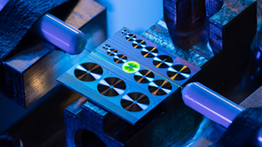 |
| An erbium-doped waveguide amplifier on a photonic integrated chip in 1X1 cm2 size, with green emission from excited erbium ions. CREDIT EPFL Laboratory of Photonics and Quantum Measurements (LPQM)/Niels Ackermann. |
Abstract:
Erbium-doped fiber amplifiers (EDFAs) are devices that can provide gain to the optical signal power in optical fibers, often used in long-distance communication fiber optic cables and fiber-based lasers. Invented in the 1980s, EDFAs are arguably one of the most important inventions, and have profoundly impacted our information society enabling signals to be routed across the Atlantic and replacing electrical repeaters.
Photonic integrated erbium doped amplifiers reach commercial performance: Boosting light power revolutionizes communications and autopilots
Lausanne, Switzerland | Posted on June 17th, 2022What is interesting about erbium ions in optical communications is that they can amplify light in the 1.55 mm wavelength region, which is where silica-based optical fibers have the lowest transmission loss. The unique electronic intra-4-f shell structure of erbium � and rare-earth ions in general � enables long-lived excited states when doped inside host materials such as glass. This provides an ideal gain medium for simultaneous amplification of multiple information-carrying channels, with negligible cross-talk, high temperature stability and low noise figure.
Optical amplification is also used in virtually all laser applications, from fiber sensing and frequency metrology, to industrial applications including laser-machining and LiDAR. Today, optical amplifiers based on rare-earth ions have become the workhorse for optical frequency combs (2005 Nobel Prize in Physics), which are used to create the world�s most precise atomic clocks.
Achieving light amplification with rare-earth ions in photonic integrated circuit can transform integrated photonics. Already in the 1990s, Bell Laboratories were looking into erbium-doped waveguide amplifiers (EDWAs), but ultimately abandoned them because their gain and output power could not match fiber-based amplifiers, while their fabrication doesn�t work with contemporary photonic integration manufacturing techniques.
Even with the recent rise of integrated photonics, renewed efforts on EDWAs have only been able to achieve less than 1 mW output power, which is not enough for many practical applications. The problem here has been high waveguide background loss, high cooperative upconversion � a gain-limiting factor at high erbium concentration, or the long-standing challenge in achieving meter-scale waveguide lengths in compact photonic chips.
Now, researchers at EPFL, led by Professor Tobias J. Kippenberg, have built an EDWA based on silicon nitride (Si3N4) photonic integrated circuits of a length up to half meter on a millimeter-scale footprint, generating a record output power of more than 145 mW and providing a small-signal net gain above 30 dB, which translates to over 1000-fold amplification in the telecommunication band in continuous operation. This performance matches the commercial, high-end EDFAs, as well as state-of-the-art heterogeneously integrated III-V semiconductor amplifiers in silicon photonics.
�We overcame the longstanding challenge by applying ion implantation � a wafer-scale process that benefits from very low cooperative upconversion even at a very high ion concentration � to the ultralow-loss silicon nitride integrated photonic circuits,� says Dr Yang Liu, a researcher in Kippenberg�s lab, and the study�s lead scientist.
�This approach allows us to achieve low loss, high erbium concentration, and a large mode-ion overlap factor in compact waveguides with meter-scale lengths, which have previously remained unsolved for decades,� says Zheru Qiu, a PhD student and co-author of the study.
�Operating with high output power and high gain is not a mere academic achievement; in fact, it is crucial to the practical operation of any amplifier, as it implies that any input signals can reach the power levels that are sufficient for long-distance high-speed data transmission and shot-noise limited detection; it also signals that high-pulse-energy femtosecond-lasers on a chip can finally become possible using this approach,� says Kippenberg.
The breakthrough signals a renaissance of rare-earth ions as viable gain media in integrated photonics, as applications of EDWAs are virtually unlimited, from optical communications and LiDAR for autonomous driving, to quantum sensing and memories for large quantum networks. It is expected to trigger follow-up studies that cover even more rare-earth ions, offering optical gain from the visible up to the mid-infrared part of the spectrum and even higher output power.
####
For more information, please click here
Contacts:
Media Contact
Nik Papageorgiou
Ecole Polytechnique F�d�rale de Lausanne
Office: 41-216-932-105
Expert Contact
Tobias J. Kippenberg
Ecole Polytechnique F�d�rale de Lausanne
Office: +41 21 693 44 28
Copyright © Ecole Polytechnique F�d�rale de Lausanne
If you have a comment, please Contact us.Issuers of news releases, not 7th Wave, Inc. or Nanotechnology Now, are solely responsible for the accuracy of the content.
Bookmark:


| Related Links |
| Related News Press |
News and information
![]() Quantum computer improves AI predictions April 17th, 2026
Quantum computer improves AI predictions April 17th, 2026
![]() Flexible sensor gains sensitivity under pressure April 17th, 2026
Flexible sensor gains sensitivity under pressure April 17th, 2026
![]() A reusable chip for particulate matter sensing April 17th, 2026
A reusable chip for particulate matter sensing April 17th, 2026
![]() Detecting vibrational quantum beating in the predissociation dynamics of SF6 using time-resolved photoelectron spectroscopy April 17th, 2026
Detecting vibrational quantum beating in the predissociation dynamics of SF6 using time-resolved photoelectron spectroscopy April 17th, 2026
Wireless/telecommunications/RF/Antennas/Microwaves
![]() Researchers develop molecular qubits that communicate at telecom frequencies October 3rd, 2025
Researchers develop molecular qubits that communicate at telecom frequencies October 3rd, 2025
Quantum communication
![]() Next-generation quantum communication October 3rd, 2025
Next-generation quantum communication October 3rd, 2025
![]() Nanophotonic platform boosts efficiency of nonlinear-optical quantum teleportation April 25th, 2025
Nanophotonic platform boosts efficiency of nonlinear-optical quantum teleportation April 25th, 2025
![]() Physicists unlock the secret of elusive quantum negative entanglement entropy using simple classical hardware August 16th, 2024
Physicists unlock the secret of elusive quantum negative entanglement entropy using simple classical hardware August 16th, 2024
Possible Futures
![]() A fundamentally new therapeutic approach to cystic fibrosis: Nanobody repairs cellular defect April 17th, 2026
A fundamentally new therapeutic approach to cystic fibrosis: Nanobody repairs cellular defect April 17th, 2026
![]() UC Irvine physicists discover method to reverse �quantum scrambling� : The work addresses the problem of information loss in quantum computing system April 17th, 2026
UC Irvine physicists discover method to reverse �quantum scrambling� : The work addresses the problem of information loss in quantum computing system April 17th, 2026
Optical computing/Photonic computing
![]() ICFO researchers overcome long-standing bottleneck in single photon detection with twisted 2D materials August 8th, 2025
ICFO researchers overcome long-standing bottleneck in single photon detection with twisted 2D materials August 8th, 2025
![]() Programmable electron-induced color router array May 14th, 2025
Programmable electron-induced color router array May 14th, 2025
Sensors
![]() Flexible sensor gains sensitivity under pressure April 17th, 2026
Flexible sensor gains sensitivity under pressure April 17th, 2026
![]() Tiny nanosheets, big leap: A new sensor detects ethanol at ultra-low levels January 30th, 2026
Tiny nanosheets, big leap: A new sensor detects ethanol at ultra-low levels January 30th, 2026
![]() From sensors to smart systems: the rise of AI-driven photonic noses January 30th, 2026
From sensors to smart systems: the rise of AI-driven photonic noses January 30th, 2026
![]() Sensors innovations for smart lithium-based batteries: advancements, opportunities, and potential challenges August 8th, 2025
Sensors innovations for smart lithium-based batteries: advancements, opportunities, and potential challenges August 8th, 2025
Announcements
![]() A fundamentally new therapeutic approach to cystic fibrosis: Nanobody repairs cellular defect April 17th, 2026
A fundamentally new therapeutic approach to cystic fibrosis: Nanobody repairs cellular defect April 17th, 2026
![]() UC Irvine physicists discover method to reverse �quantum scrambling� : The work addresses the problem of information loss in quantum computing system April 17th, 2026
UC Irvine physicists discover method to reverse �quantum scrambling� : The work addresses the problem of information loss in quantum computing system April 17th, 2026
Photonics/Optics/Lasers
![]() Metasurfaces smooth light to boost magnetic sensing precision January 30th, 2026
Metasurfaces smooth light to boost magnetic sensing precision January 30th, 2026
![]() From sensors to smart systems: the rise of AI-driven photonic noses January 30th, 2026
From sensors to smart systems: the rise of AI-driven photonic noses January 30th, 2026
|
|
||
|
|
||
| The latest news from around the world, FREE | ||
|
|
||
|
|
||
| Premium Products | ||
|
|
||
|
Only the news you want to read!
Learn More |
||
|
|
||
|
Full-service, expert consulting
Learn More |
||
|
|
||