Home > Press > More sensitive X-ray imaging: Improvements in the material that converts X-rays into light, for medical or industrial images, could allow a tenfold signal enhancement
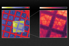 |
| Researchers at MIT have shown how one could improve the efficiency of scintillators by at least tenfold by changing the material’s surface. This image shows a TEM grid on scotch tape, with the right side showing the scene after it is corrected. CREDIT Image courtesy of Charles Roques-Carmes, Nicholas Rivera, Marin Soljacic, Steven Johnson, and John Joannopoulos, et al |
Abstract:
Scintillators are materials that emit light when bombarded with high-energy particles or X-rays. In medical or dental X-ray systems, they convert incoming X-ray radiation into visible light that can then be captured using film or photosensors. They’re also used for night-vision systems and for research, such as in particle detectors or electron microscopes.
More sensitive X-ray imaging: Improvements in the material that converts X-rays into light, for medical or industrial images, could allow a tenfold signal enhancement
Cambridge, MA | Posted on February 25th, 2022Researchers at MIT have now shown how one could improve the efficiency of scintillators by at least tenfold, and perhaps even a hundredfold, by changing the material’s surface to create certain nanoscale configurations, such as arrays of wave-like ridges. While past attempts to develop more efficient scintillators have focused on finding new materials, the new approach could in principle work with any of the existing materials.
Though it will require more time and effort to integrate their scintillators into existing X-ray machines, the team believes that this method might lead to improvements in medical diagnostic X-rays or CT scans, to reduce dose exposure and improve image quality. In other applications, such as X-ray inspection of manufactured parts for quality control, the new scintillators could enable inspections with higher accuracy or at faster speeds.
The findings are described in the journal Science, in a paper by MIT doctoral students Charles Roques-Carmes and Nicholas Rivera; MIT professors Marin Soljacic, Steven Johnson, and John Joannopoulos; and 10 others.
While scintillators have been in use for some 70 years, much of the research in the field has focused on developing new materials that produce brighter or faster light emissions. The new approach instead applies advances in nanotechnology to existing materials. By creating patterns in scintillator materials at a length scale comparable to the wavelengths of the light being emitted, the team found that it was possible to dramatically change the material’s optical properties.
To make what they coined “nanophotonic scintillators,” Roques-Carmes says, “you can directly make patterns inside the scintillators, or you can glue on another material that would have holes on the nanoscale. The specifics depend on the exact structure and material.” For this research, the team took a scintillator and made holes spaced apart by roughly one optical wavelength, or about 500 nanometers (billionths of a meter).
“The key to what we’re doing is a general theory and framework we have developed,” Rivera says. This allows the researchers to calculate the scintillation levels that would be produced by any arbitrary configuration of nanophotonic structures. The scintillation process itself involves a series of steps, making it complicated to unravel. The framework the team developed involves integrating three different types of physics, Roques-Carmes says. Using this system they have found a good match between their predictions and the results of their subsequent experiments.
The experiments showed a tenfold improvement in emission from the treated scintillator. “So, this is something that might translate into applications for medical imaging, which are optical photon-starved, meaning the conversion of X-rays to optical light limits the image quality. [In medical imaging,] you do not want to irradiate your patients with too much of the X-rays, especially for routine screening, and especially for young patients as well,” Roques-Carmes says.
“We believe that this will open a new field of research in nanophotonics,” he adds. “You can use a lot of the existing work and research that has been done in the field of nanophotonics to improve significantly on existing materials that scintillate.”
Soljacic says that while their experiments proved a tenfold improvement in emission could be achieved, by further fine-tuning the design of the nanoscale patterning, “we also show that you can get up to 100 times [improvement], and we believe we also have a path toward making it even better,” he says.
Soljacic points out that in other areas of nanophotonics, a field that deals with how light interacts with materials that are structured at the nanometer scale, the development of computational simulations has enabled rapid, substantial improvements, for example in the development of solar cells and LEDs. The new models this team developed for scintillating materials could facilitate similar leaps in this technology, he says.
Nanophotonics techniques “give you the ultimate power of tailoring and enhancing the behavior of light,” Soljacic says. “But until now, this promise, this ability to do this with scintillation was unreachable because modeling the scintillation was very challenging. Now, this work for the first time opens up this field of scintillation, fully opens it, for the application of nanophotonics techniques.” More generally, the team believes that the combination of nanophotonic and scintillators might ultimately enable higher resolution, reduced X-ray dose, and energy-resolved X-ray imaging.
Yablonovitch adds that while the concept still needs to be proven in a practical device, he says that, “After years of research on photonic crystals in optical communication and other fields, it's long overdue that photonic crystals should be applied to scintillators, which are of great practical importance yet have been overlooked” until this work.
The research team included Ali Ghorashi, Steven Kooi, Yi Yang, Zin Lin, Justin Beroz, Aviram Massuda, Jamison Sloan, and Nicolas Romeo at MIT; Yang Yu at Raith America, Inc.; and Ido Kaminer at Technion in Israel. The work was supported, in part, by the U.S. Army Research Office and the U.S. Army Research Laboratory through the Institute for Soldier Nanotechnologies, by the Air Force Office of Scientific Research, and by a Mathworks Engineering Fellowship.
###
Written by David Chandler, MIT News Office
####
For more information, please click here
Contacts:
Abby Abazorius
Massachusetts Institute of Technology
Office: 617-253-2709
Copyright © Massachusetts Institute of Technology
If you have a comment, please Contact us.Issuers of news releases, not 7th Wave, Inc. or Nanotechnology Now, are solely responsible for the accuracy of the content.
Bookmark:


| Related Links |
| Related News Press |
News and information
![]() Quantum computer improves AI predictions April 17th, 2026
Quantum computer improves AI predictions April 17th, 2026
![]() Flexible sensor gains sensitivity under pressure April 17th, 2026
Flexible sensor gains sensitivity under pressure April 17th, 2026
![]() A reusable chip for particulate matter sensing April 17th, 2026
A reusable chip for particulate matter sensing April 17th, 2026
![]() Detecting vibrational quantum beating in the predissociation dynamics of SF6 using time-resolved photoelectron spectroscopy April 17th, 2026
Detecting vibrational quantum beating in the predissociation dynamics of SF6 using time-resolved photoelectron spectroscopy April 17th, 2026
Imaging
![]() Simple algorithm paired with standard imaging tool could predict failure in lithium metal batteries August 8th, 2025
Simple algorithm paired with standard imaging tool could predict failure in lithium metal batteries August 8th, 2025
Possible Futures
![]() A fundamentally new therapeutic approach to cystic fibrosis: Nanobody repairs cellular defect April 17th, 2026
A fundamentally new therapeutic approach to cystic fibrosis: Nanobody repairs cellular defect April 17th, 2026
![]() UC Irvine physicists discover method to reverse ‘quantum scrambling’ : The work addresses the problem of information loss in quantum computing system April 17th, 2026
UC Irvine physicists discover method to reverse ‘quantum scrambling’ : The work addresses the problem of information loss in quantum computing system April 17th, 2026
Nanomedicine
![]() A fundamentally new therapeutic approach to cystic fibrosis: Nanobody repairs cellular defect April 17th, 2026
A fundamentally new therapeutic approach to cystic fibrosis: Nanobody repairs cellular defect April 17th, 2026
![]() New molecular technology targets tumors and simultaneously silences two ‘undruggable’ cancer genes August 8th, 2025
New molecular technology targets tumors and simultaneously silences two ‘undruggable’ cancer genes August 8th, 2025
![]() New imaging approach transforms study of bacterial biofilms August 8th, 2025
New imaging approach transforms study of bacterial biofilms August 8th, 2025
![]() Electrifying results shed light on graphene foam as a potential material for lab grown cartilage June 6th, 2025
Electrifying results shed light on graphene foam as a potential material for lab grown cartilage June 6th, 2025
Discoveries
![]() Quantum computer improves AI predictions April 17th, 2026
Quantum computer improves AI predictions April 17th, 2026
![]() Flexible sensor gains sensitivity under pressure April 17th, 2026
Flexible sensor gains sensitivity under pressure April 17th, 2026
![]() A reusable chip for particulate matter sensing April 17th, 2026
A reusable chip for particulate matter sensing April 17th, 2026
![]() Detecting vibrational quantum beating in the predissociation dynamics of SF6 using time-resolved photoelectron spectroscopy April 17th, 2026
Detecting vibrational quantum beating in the predissociation dynamics of SF6 using time-resolved photoelectron spectroscopy April 17th, 2026
Announcements
![]() A fundamentally new therapeutic approach to cystic fibrosis: Nanobody repairs cellular defect April 17th, 2026
A fundamentally new therapeutic approach to cystic fibrosis: Nanobody repairs cellular defect April 17th, 2026
![]() UC Irvine physicists discover method to reverse ‘quantum scrambling’ : The work addresses the problem of information loss in quantum computing system April 17th, 2026
UC Irvine physicists discover method to reverse ‘quantum scrambling’ : The work addresses the problem of information loss in quantum computing system April 17th, 2026
Interviews/Book Reviews/Essays/Reports/Podcasts/Journals/White papers/Posters
![]() A fundamentally new therapeutic approach to cystic fibrosis: Nanobody repairs cellular defect April 17th, 2026
A fundamentally new therapeutic approach to cystic fibrosis: Nanobody repairs cellular defect April 17th, 2026
![]() UC Irvine physicists discover method to reverse ‘quantum scrambling’ : The work addresses the problem of information loss in quantum computing system April 17th, 2026
UC Irvine physicists discover method to reverse ‘quantum scrambling’ : The work addresses the problem of information loss in quantum computing system April 17th, 2026
Military
![]() Quantum engineers ‘squeeze’ laser frequency combs to make more sensitive gas sensors January 17th, 2025
Quantum engineers ‘squeeze’ laser frequency combs to make more sensitive gas sensors January 17th, 2025
![]() Chainmail-like material could be the future of armor: First 2D mechanically interlocked polymer exhibits exceptional flexibility and strength January 17th, 2025
Chainmail-like material could be the future of armor: First 2D mechanically interlocked polymer exhibits exceptional flexibility and strength January 17th, 2025
![]() Single atoms show their true color July 5th, 2024
Single atoms show their true color July 5th, 2024
![]() NRL charters Navy’s quantum inertial navigation path to reduce drift April 5th, 2024
NRL charters Navy’s quantum inertial navigation path to reduce drift April 5th, 2024
|
|
||
|
|
||
| The latest news from around the world, FREE | ||
|
|
||
|
|
||
| Premium Products | ||
|
|
||
|
Only the news you want to read!
Learn More |
||
|
|
||
|
Full-service, expert consulting
Learn More |
||
|
|
||