Home > Press > Redrawing the lines: Growing inexpensive, high-quality iron-based superconductors: Regions of different crystalline orientation in superconductors can be manipulated in a simple and scalable manner to improve their properties
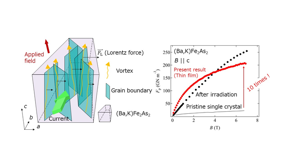 |
| Schematic illustration of how vortices are pinned by low-angle grain boundaries in a (Ba,K)Fe2As2 superconductor. The pinning force density Fp of (Ba,K)Fe2As2 thin film fabricated in this study is almost 10 times as high as a pristine single crystal. CREDIT Kazumasa Iida |
Abstract:
Superconducting materials show zero electrical resistance at low temperatures, which allows them to conduct “supercurrents” without dissipation. Recently, a group of scientists led by Dr. Kazumasa Iida from Nagoya University, Japan, developed an inexpensive, scalable way to produce high-temperature superconductors using “grain boundary engineering” techniques. The new method could help develop stronger, inexpensive, and high operating temperature superconductors with impactful technological applications.
Redrawing the lines: Growing inexpensive, high-quality iron-based superconductors: Regions of different crystalline orientation in superconductors can be manipulated in a simple and scalable manner to improve their properties
Nagoya, Japan | Posted on December 17th, 2021Key to the dissipation-free conduction of currents in superconductors in the presence of a magnetic field is a property called “pinning potential.” Pinning describes how defects in the superconducting matrix pin vortices against the Lorentz force. Controlling the micro-structure of the material allows for careful introduction of defects into the material to form “artificial pinning centers” (APCs), which can then improve its properties. The most common approach to introducing such defects into superconductors is “ion irradiation.” However, ion irradiation is both complicated and expensive.
In their study published in NPG Asia Materials, Professor Iida and his research team successfully grew a thin film superconductor that has a surprisingly high pinning efficiency without APCs. “Crystalline materials are made up of different regions with different crystalline orientations called ‘grains.’ When the angle between the boundaries of different grains in the material are less than their critical angle, θc, we call it a ‘low-angle grain boundary (LAGB).’ LAGBs contribute to magnetic flux pinning, which enhances the properties of the superconductor,” explains Dr. Iida.
Iron (Fe)-based superconductors (FBS) are considered to be the next-generation superconductor technology. In their study, Professor Iida and team grew an FBS called “potassium (K)-doped BaFe2As2 (Ba122)” using a technique called “molecular beam epitaxy,” in which the superconductor is grown on a substrate. “The difficulties involved in controlling volatile potassium made the realization of epitaxial K-doped Ba122 challenging, but we succeeded in growing the thin films on fluoride substrates,” says Dr. Iida.
The team then characterized the FBS using transmission electron microscopy and found that the film was composed of columnar grains approximately 30–60 nm wide. These grains were rotated around the crystallographic principle axes by angles well within θc for K-doped Ba122 and formed LAGB networks.
The researchers then performed measurements of the thin film’s electrical resistivity and magnetic properties. They observed that the thin films had a surprisingly high critical current (the maximum current in a superconductor above which it transitions to a dissipation state). The LAGB networks further ensured a strong pinning efficiency in the material. “The in-field properties obtained in our study are comparable to that of ion-irradiated K-doped Ba122. Moreover, grain boundary engineering is a simple technique and can be scaled up for industrial applications,” comments Dr. Iida.
The findings of this study could accelerate the development of strong magnets using superconductors, leading to advances in magnetic resonance imaging (MRI). The widespread application of MRI is currently limited by the high investment and operational cost of the MRI machines due to the cooling costs of the superconductors within. But with simple and inexpensive techniques such as grain boundary engineering for fabricating superconductors, MRIs could become more accessible to patients, improving our quality of life.
Funding information:
This work was supported by JST CREST Grant number JPMJCR18J4.
####
For more information, please click here
Contacts:
Naomi Inoue
Nagoya University
Expert Contact
Kazumasa Iida
Nagoya University
Copyright © Nagoya University
If you have a comment, please Contact us.Issuers of news releases, not 7th Wave, Inc. or Nanotechnology Now, are solely responsible for the accuracy of the content.
Bookmark:


| Related Links |
| Related News Press |
News and information
![]() Decoding hydrogen‑bond network of electrolyte for cryogenic durable aqueous zinc‑ion batteries January 30th, 2026
Decoding hydrogen‑bond network of electrolyte for cryogenic durable aqueous zinc‑ion batteries January 30th, 2026
![]() COF scaffold membrane with gate‑lane nanostructure for efficient Li+/Mg2+ separation January 30th, 2026
COF scaffold membrane with gate‑lane nanostructure for efficient Li+/Mg2+ separation January 30th, 2026
Superconductivity
![]() MXene nanomaterials enter a new dimension Multilayer nanomaterial: MXene flakes created at Drexel University show new promise as 1D scrolls January 30th, 2026
MXene nanomaterials enter a new dimension Multilayer nanomaterial: MXene flakes created at Drexel University show new promise as 1D scrolls January 30th, 2026
![]() Lattice-driven charge density wave fluctuations far above the transition temperature in Kagome superconductor April 25th, 2025
Lattice-driven charge density wave fluctuations far above the transition temperature in Kagome superconductor April 25th, 2025
Possible Futures
![]() Decoding hydrogen‑bond network of electrolyte for cryogenic durable aqueous zinc‑ion batteries January 30th, 2026
Decoding hydrogen‑bond network of electrolyte for cryogenic durable aqueous zinc‑ion batteries January 30th, 2026
![]() COF scaffold membrane with gate‑lane nanostructure for efficient Li+/Mg2+ separation January 30th, 2026
COF scaffold membrane with gate‑lane nanostructure for efficient Li+/Mg2+ separation January 30th, 2026
Discoveries
![]() From sensors to smart systems: the rise of AI-driven photonic noses January 30th, 2026
From sensors to smart systems: the rise of AI-driven photonic noses January 30th, 2026
![]() Decoding hydrogen‑bond network of electrolyte for cryogenic durable aqueous zinc‑ion batteries January 30th, 2026
Decoding hydrogen‑bond network of electrolyte for cryogenic durable aqueous zinc‑ion batteries January 30th, 2026
![]() COF scaffold membrane with gate‑lane nanostructure for efficient Li+/Mg2+ separation January 30th, 2026
COF scaffold membrane with gate‑lane nanostructure for efficient Li+/Mg2+ separation January 30th, 2026
Announcements
![]() Decoding hydrogen‑bond network of electrolyte for cryogenic durable aqueous zinc‑ion batteries January 30th, 2026
Decoding hydrogen‑bond network of electrolyte for cryogenic durable aqueous zinc‑ion batteries January 30th, 2026
![]() COF scaffold membrane with gate‑lane nanostructure for efficient Li+/Mg2+ separation January 30th, 2026
COF scaffold membrane with gate‑lane nanostructure for efficient Li+/Mg2+ separation January 30th, 2026
Interviews/Book Reviews/Essays/Reports/Podcasts/Journals/White papers/Posters
![]() Metasurfaces smooth light to boost magnetic sensing precision January 30th, 2026
Metasurfaces smooth light to boost magnetic sensing precision January 30th, 2026
![]() COF scaffold membrane with gate‑lane nanostructure for efficient Li+/Mg2+ separation January 30th, 2026
COF scaffold membrane with gate‑lane nanostructure for efficient Li+/Mg2+ separation January 30th, 2026
|
|
||
|
|
||
| The latest news from around the world, FREE | ||
|
|
||
|
|
||
| Premium Products | ||
|
|
||
|
Only the news you want to read!
Learn More |
||
|
|
||
|
Full-service, expert consulting
Learn More |
||
|
|
||