Home > Press > Stress-free path to stress-free metallic films paves the way for next-gen circuitry: Optimized sputtering technique helps minimize stress in tungsten thin films
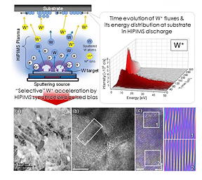 |
| (top left) An illustration of the HiPIMS process (top right) The energy distribution of tungsten ions arriving at the substrate over time. At short times, there are a large proportion of ions with high energy. (bottom) Stress-free tungsten films created with the selective pulsed bias technique. (a) Plan view transmission electron microscopy (TEM) image of the film; (b) a higher resolution image; (c) reconstructions of the selected area in (b) based on inverse Fourier transforms, with two regions magnified. CREDIT Tokyo Metropolitan University |
Abstract:
Researchers from Tokyo Metropolitan University have used high power impulse magnetron scattering (HiPIMS) to create thin films of tungsten with unprecedentedly low levels of film stress. By optimizing the timing of a "substrate bias pulse" with microsecond precision, they minimized impurities and defects to form crystalline films with stresses as low as 0.03 GPa, similar to those achieved through annealing. Their work promises efficient pathways for creating metallic films for the electronics industry.
Stress-free path to stress-free metallic films paves the way for next-gen circuitry: Optimized sputtering technique helps minimize stress in tungsten thin films
Tokyo, Japan | Posted on July 4th, 2021Modern electronics relies on the intricate, nanoscale deposition of thin metallic films onto surfaces. This is easier said than done; unless done right, "film stresses" arising from the microscopic internal structure of the film can cause buckling and curving over time. Getting rid of these stresses usually requires heating or "annealing". Unfortunately, many of the best metals for the job e.g. tungsten have high melting points, meaning that the film needs to be heated to over 1000 degrees Celsius. Not only is this energy intensive, but it severely limits which substrate materials can be used. The race is on to create films out of high melting point metals without these stresses in the first place.
A team led by Associate Professor Tetsuhide Shimizu of Tokyo Metropolitan University have been working with a technique known as high power impulse magnetron scattering (HiPIMS), a sputtering technique. Sputtering involves applying a high voltage across a metallic "target" and a substrate, creating a plasma of charged gas atoms which bombards the metallic target and forms a charged metal vapor; these metal ions fly towards the substrate where they form a film. In the case of HiPIMS, the voltage is pulsed in short, powerful bursts. After each pulse, it is known that there is some separation between the arrival of metal and gas ions at the substrate; a synchronized "substrate bias" pulse can help selectively accelerate the metal ions, creating denser films. Yet despite many efforts, the issue of residual stress remained.
Now, using argon gas and a tungsten target, the team looked at how ions with different energies arrived at the substrate over time in unprecedented detail. Instead of using a bias pulse set off at the same time as the HiPIMS pulse, they used their knowledge of when different ions arrived and introduced a tiny delay, 60 microseconds, to precisely select for the arrival of high energy metal ions. They found that this minimized the amount of gas ending up in the film and efficiently delivered high levels of kinetic energy. The result was a dense crystalline film with large grains and low film stress. By making the bias stronger, the films became more and more stress-free. The efficient delivery of energy to the film meant that they had, in fact, achieved a similar effect to annealing while they deposited the film. By further swapping out argon for krypton, the team realized films with a stress as low as 0.03 GPa, comparable to what can be made with post-annealing.
An efficient pathway to stress-free films will have a significant impact on metallization processes and the manufacture of next-generation circuitry. The technology may be applied to other metals and promises big gains for the electronics industry.
###
This work was supported by the Fund for the Promotion of Joint International Research (No.17KK0136) of the Japan Society for the Promotion of Science (JSPS), the Swedish Research Council (No. VR 2018-04139), and the Swedish Government Strategic Research Area in Materials Science on Functional Materials at Link�ping University (Faculty Grant SFO-Mat-LiU No. 2009-00971).
####
For more information, please click here
Contacts:
Go Totsukawa
81-426-772-728
@TMU_PR
Copyright © Tokyo Metropolitan University
If you have a comment, please Contact us.Issuers of news releases, not 7th Wave, Inc. or Nanotechnology Now, are solely responsible for the accuracy of the content.
Bookmark:


| Related Links |
| Related News Press |
News and information
![]() Quantum computer improves AI predictions April 17th, 2026
Quantum computer improves AI predictions April 17th, 2026
![]() Flexible sensor gains sensitivity under pressure April 17th, 2026
Flexible sensor gains sensitivity under pressure April 17th, 2026
![]() A reusable chip for particulate matter sensing April 17th, 2026
A reusable chip for particulate matter sensing April 17th, 2026
![]() Detecting vibrational quantum beating in the predissociation dynamics of SF6 using time-resolved photoelectron spectroscopy April 17th, 2026
Detecting vibrational quantum beating in the predissociation dynamics of SF6 using time-resolved photoelectron spectroscopy April 17th, 2026
Thin films
![]() Tiny nanosheets, big leap: A new sensor detects ethanol at ultra-low levels January 30th, 2026
Tiny nanosheets, big leap: A new sensor detects ethanol at ultra-low levels January 30th, 2026
![]() Utilizing palladium for addressing contact issues of buried oxide thin film transistors April 5th, 2024
Utilizing palladium for addressing contact issues of buried oxide thin film transistors April 5th, 2024
![]() Understanding the mechanism of non-uniform formation of diamond film on tools: Paving the way to a dry process with less environmental impact March 24th, 2023
Understanding the mechanism of non-uniform formation of diamond film on tools: Paving the way to a dry process with less environmental impact March 24th, 2023
![]() New study introduces the best graphite films: The work by Distinguished Professor Feng Ding at UNIST has been published in the October 2022 issue of Nature Nanotechnology November 4th, 2022
New study introduces the best graphite films: The work by Distinguished Professor Feng Ding at UNIST has been published in the October 2022 issue of Nature Nanotechnology November 4th, 2022
Govt.-Legislation/Regulation/Funding/Policy
![]() Quantum computer improves AI predictions April 17th, 2026
Quantum computer improves AI predictions April 17th, 2026
![]() Metasurfaces smooth light to boost magnetic sensing precision January 30th, 2026
Metasurfaces smooth light to boost magnetic sensing precision January 30th, 2026
![]() New imaging approach transforms study of bacterial biofilms August 8th, 2025
New imaging approach transforms study of bacterial biofilms August 8th, 2025
Possible Futures
![]() A fundamentally new therapeutic approach to cystic fibrosis: Nanobody repairs cellular defect April 17th, 2026
A fundamentally new therapeutic approach to cystic fibrosis: Nanobody repairs cellular defect April 17th, 2026
![]() UC Irvine physicists discover method to reverse �quantum scrambling� : The work addresses the problem of information loss in quantum computing system April 17th, 2026
UC Irvine physicists discover method to reverse �quantum scrambling� : The work addresses the problem of information loss in quantum computing system April 17th, 2026
Chip Technology
![]() A reusable chip for particulate matter sensing April 17th, 2026
A reusable chip for particulate matter sensing April 17th, 2026
![]() Metasurfaces smooth light to boost magnetic sensing precision January 30th, 2026
Metasurfaces smooth light to boost magnetic sensing precision January 30th, 2026
Discoveries
![]() Quantum computer improves AI predictions April 17th, 2026
Quantum computer improves AI predictions April 17th, 2026
![]() Flexible sensor gains sensitivity under pressure April 17th, 2026
Flexible sensor gains sensitivity under pressure April 17th, 2026
![]() A reusable chip for particulate matter sensing April 17th, 2026
A reusable chip for particulate matter sensing April 17th, 2026
![]() Detecting vibrational quantum beating in the predissociation dynamics of SF6 using time-resolved photoelectron spectroscopy April 17th, 2026
Detecting vibrational quantum beating in the predissociation dynamics of SF6 using time-resolved photoelectron spectroscopy April 17th, 2026
Materials/Metamaterials/Magnetoresistance
![]() First real-time observation of two-dimensional melting process: Researchers at Mainz University unveil new insights into magnetic vortex structures August 8th, 2025
First real-time observation of two-dimensional melting process: Researchers at Mainz University unveil new insights into magnetic vortex structures August 8th, 2025
![]() Researchers unveil a groundbreaking clay-based solution to capture carbon dioxide and combat climate change June 6th, 2025
Researchers unveil a groundbreaking clay-based solution to capture carbon dioxide and combat climate change June 6th, 2025
![]() A 1960s idea inspires NBI researchers to study hitherto inaccessible quantum states June 6th, 2025
A 1960s idea inspires NBI researchers to study hitherto inaccessible quantum states June 6th, 2025
![]() Institute for Nanoscience hosts annual proposal planning meeting May 16th, 2025
Institute for Nanoscience hosts annual proposal planning meeting May 16th, 2025
Announcements
![]() A fundamentally new therapeutic approach to cystic fibrosis: Nanobody repairs cellular defect April 17th, 2026
A fundamentally new therapeutic approach to cystic fibrosis: Nanobody repairs cellular defect April 17th, 2026
![]() UC Irvine physicists discover method to reverse �quantum scrambling� : The work addresses the problem of information loss in quantum computing system April 17th, 2026
UC Irvine physicists discover method to reverse �quantum scrambling� : The work addresses the problem of information loss in quantum computing system April 17th, 2026
Grants/Sponsored Research/Awards/Scholarships/Gifts/Contests/Honors/Records
![]() Quantum computer improves AI predictions April 17th, 2026
Quantum computer improves AI predictions April 17th, 2026
![]() Detecting vibrational quantum beating in the predissociation dynamics of SF6 using time-resolved photoelectron spectroscopy April 17th, 2026
Detecting vibrational quantum beating in the predissociation dynamics of SF6 using time-resolved photoelectron spectroscopy April 17th, 2026
![]() Metasurfaces smooth light to boost magnetic sensing precision January 30th, 2026
Metasurfaces smooth light to boost magnetic sensing precision January 30th, 2026
Research partnerships
![]() Lab to industry: InSe wafer-scale breakthrough for future electronics August 8th, 2025
Lab to industry: InSe wafer-scale breakthrough for future electronics August 8th, 2025
![]() HKU physicists uncover hidden order in the quantum world through deconfined quantum critical points April 25th, 2025
HKU physicists uncover hidden order in the quantum world through deconfined quantum critical points April 25th, 2025
|
|
||
|
|
||
| The latest news from around the world, FREE | ||
|
|
||
|
|
||
| Premium Products | ||
|
|
||
|
Only the news you want to read!
Learn More |
||
|
|
||
|
Full-service, expert consulting
Learn More |
||
|
|
||