Home > Press > 2D materials for conducting hole currents from grain boundaries in perovskite solar cells
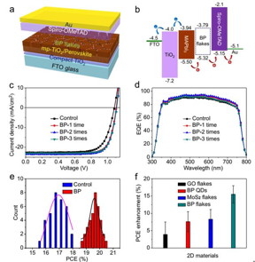 |
| a,b The structural schematic diagram and energy-level band diagram of a BP-modified PSC with a normal structure. c,d Current density-voltage (J-V) curves (reverse scan) and external quantum efficiency (EQE) spectra of PSCs without (control) and with BP deposition (1~3 times) on perovskite film surface. e Histogram of power conversion efficiencies (PCEs) of PSCs without (control) and with BP modification (BP coating for 2 times). The PCEs are derived from the reverse scans of the J-V curves. f The average PCE enhancement after the modification of perovskite films with different 2-D materials. CREDIT by Peng You, Guanqi Tang, Jiupeng Cao, Dong Shen, Tsz-Wai Ng, Zafer Hawash, Naixiang Wang, Chun-Ki Liu, Wei Lu, Qidong Tai, Yabing Qi, Chun-Sing Lee, Feng Yan |
Abstract:
Grain boundaries (GBs) in PSCs have been found to be detrimental to the photovoltaic performance of the devices. Numerous papers reported that the defects in perovskite GBs should be passivated by suitable materials, such as quaternary ammonium halide, fullerene derivatives and CH3NH3I, to alleviate carrier recombination and consequently improve the device performance.
2D materials for conducting hole currents from grain boundaries in perovskite solar cells
Changchun, China | Posted on April 2nd, 2021In a new paper published in Light: Science & Applications, a team of scientists, led by Professor Feng Yan from Department of Applied Physics, The Hong Kong Polytechnic University, Hung Hom, Kowloon, Hong Kong, and co-workers have developed a novel method to overcome the drawback of perovskite GBs without defect passivation on them. Several 2-D materials, including black phosphorus (BP), MoS2 and graphene oxide (GO), are specifically modified on the edge of perovskite GBs by a solution process. The 2-D materials have high carrier mobilities, ultrathin thicknesses and smooth surfaces without dangling bonds. The PCEs of the devices are substantially enhanced by the 2-D flakes, in which BP flakes can induce the highest relative enhancement of about 15%. More interestingly, they find that, under certain conditions, GBs modified with the 2-D materials are favorable for the device performance. Therefore, a synergistic effect between the 2-D flakes and perovskite GBs is observed for the first time. Although the nanotechnology of using 2-D materials in PSCs has been reported in some papers, the synergistic effect between the 2-D flakes and perovskite GBs has not been reported until now. To better understand the underlying mechanism of the above effect, device simulation was conducted by using a commercial software. The hole conduction processes from GBs to 2-D flakes in PSCs are clearly demonstrated, showing that the GBs and 2-D flakes all act as hole channels in the devices. The simulation results confirm that the performance enhancement induced by BP is higher than that by other 2-D materials because of the highest hole mobility of BP. In addition, the modification of the 2-D flakes on the perovskite grains away from GBs has little effect on the device performance, indicating that the synergistic effect of 2-D flakes and perovskite GBs is essential to the performance enhancement in our devices.
Although the coverage of the 2-D flakes on the perovskite films is only several percent, most of the flakes are located on perovskite GBs. Due to the high carrier mobilities of the 2-D materials especially BP, hole transfer from GBs is dramatically enhanced in the PSCs, resulting in substantial improvements of the efficiency as well as the stability of the devices. These results also indicate that GBs in PSCs are not detrimental to the device performance if the accumulated holes in the GBs can be conducted out efficiently. Under certain conditions, GBs even can be favorable for the photovoltaic performance of PSCs due to the built-in electric fields around them, which can facilitate photocarrier separation and transfer in the devices. Therefore, perovskite GBs are electrically benign, which is consistent with some theoretical calculations reported before. More importantly, they observed the synergic effect of the 2D flakes on the GBs in PSCs for the first time. Both the carrier mobility and the location of the 2D flakes on the perovskite surface are essential to the performance enhancement. This work provides a guideline of modifying perovskite layers with novel high-mobility 2-D materials to improve the photovoltaic performance as well as the stability of PSCs.
####
For more information, please click here
Contacts:
Feng Yan
Copyright © Changchun Institute of Optics, Fine Mechanics and Physics, Chinese Academy of Sciences
If you have a comment, please Contact us.Issuers of news releases, not 7th Wave, Inc. or Nanotechnology Now, are solely responsible for the accuracy of the content.
Bookmark:


| Related Links |
| Related News Press |
News and information
![]() Decoding hydrogen‑bond network of electrolyte for cryogenic durable aqueous zinc‑ion batteries January 30th, 2026
Decoding hydrogen‑bond network of electrolyte for cryogenic durable aqueous zinc‑ion batteries January 30th, 2026
![]() COF scaffold membrane with gate‑lane nanostructure for efficient Li+/Mg2+ separation January 30th, 2026
COF scaffold membrane with gate‑lane nanostructure for efficient Li+/Mg2+ separation January 30th, 2026
2 Dimensional Materials
![]() MXene nanomaterials enter a new dimension Multilayer nanomaterial: MXene flakes created at Drexel University show new promise as 1D scrolls January 30th, 2026
MXene nanomaterials enter a new dimension Multilayer nanomaterial: MXene flakes created at Drexel University show new promise as 1D scrolls January 30th, 2026
![]() ICFO researchers overcome long-standing bottleneck in single photon detection with twisted 2D materials August 8th, 2025
ICFO researchers overcome long-standing bottleneck in single photon detection with twisted 2D materials August 8th, 2025
![]() First real-time observation of two-dimensional melting process: Researchers at Mainz University unveil new insights into magnetic vortex structures August 8th, 2025
First real-time observation of two-dimensional melting process: Researchers at Mainz University unveil new insights into magnetic vortex structures August 8th, 2025
![]() Lab to industry: InSe wafer-scale breakthrough for future electronics August 8th, 2025
Lab to industry: InSe wafer-scale breakthrough for future electronics August 8th, 2025
Perovskites
Possible Futures
![]() Decoding hydrogen‑bond network of electrolyte for cryogenic durable aqueous zinc‑ion batteries January 30th, 2026
Decoding hydrogen‑bond network of electrolyte for cryogenic durable aqueous zinc‑ion batteries January 30th, 2026
![]() COF scaffold membrane with gate‑lane nanostructure for efficient Li+/Mg2+ separation January 30th, 2026
COF scaffold membrane with gate‑lane nanostructure for efficient Li+/Mg2+ separation January 30th, 2026
Discoveries
![]() From sensors to smart systems: the rise of AI-driven photonic noses January 30th, 2026
From sensors to smart systems: the rise of AI-driven photonic noses January 30th, 2026
![]() Decoding hydrogen‑bond network of electrolyte for cryogenic durable aqueous zinc‑ion batteries January 30th, 2026
Decoding hydrogen‑bond network of electrolyte for cryogenic durable aqueous zinc‑ion batteries January 30th, 2026
![]() COF scaffold membrane with gate‑lane nanostructure for efficient Li+/Mg2+ separation January 30th, 2026
COF scaffold membrane with gate‑lane nanostructure for efficient Li+/Mg2+ separation January 30th, 2026
Announcements
![]() Decoding hydrogen‑bond network of electrolyte for cryogenic durable aqueous zinc‑ion batteries January 30th, 2026
Decoding hydrogen‑bond network of electrolyte for cryogenic durable aqueous zinc‑ion batteries January 30th, 2026
![]() COF scaffold membrane with gate‑lane nanostructure for efficient Li+/Mg2+ separation January 30th, 2026
COF scaffold membrane with gate‑lane nanostructure for efficient Li+/Mg2+ separation January 30th, 2026
Interviews/Book Reviews/Essays/Reports/Podcasts/Journals/White papers/Posters
![]() Metasurfaces smooth light to boost magnetic sensing precision January 30th, 2026
Metasurfaces smooth light to boost magnetic sensing precision January 30th, 2026
![]() COF scaffold membrane with gate‑lane nanostructure for efficient Li+/Mg2+ separation January 30th, 2026
COF scaffold membrane with gate‑lane nanostructure for efficient Li+/Mg2+ separation January 30th, 2026
Energy
![]() Sensors innovations for smart lithium-based batteries: advancements, opportunities, and potential challenges August 8th, 2025
Sensors innovations for smart lithium-based batteries: advancements, opportunities, and potential challenges August 8th, 2025
![]() Simple algorithm paired with standard imaging tool could predict failure in lithium metal batteries August 8th, 2025
Simple algorithm paired with standard imaging tool could predict failure in lithium metal batteries August 8th, 2025
Solar/Photovoltaic
![]() Spinel-type sulfide semiconductors to operate the next-generation LEDs and solar cells For solar-cell absorbers and green-LED source October 3rd, 2025
Spinel-type sulfide semiconductors to operate the next-generation LEDs and solar cells For solar-cell absorbers and green-LED source October 3rd, 2025
![]() KAIST researchers introduce new and improved, next-generation perovskite solar cell November 8th, 2024
KAIST researchers introduce new and improved, next-generation perovskite solar cell November 8th, 2024
![]() Groundbreaking precision in single-molecule optoelectronics August 16th, 2024
Groundbreaking precision in single-molecule optoelectronics August 16th, 2024
![]() Development of zinc oxide nanopagoda array photoelectrode: photoelectrochemical water-splitting hydrogen production January 12th, 2024
Development of zinc oxide nanopagoda array photoelectrode: photoelectrochemical water-splitting hydrogen production January 12th, 2024
|
|
||
|
|
||
| The latest news from around the world, FREE | ||
|
|
||
|
|
||
| Premium Products | ||
|
|
||
|
Only the news you want to read!
Learn More |
||
|
|
||
|
Full-service, expert consulting
Learn More |
||
|
|
||