Home > Press > Light in concert with force reveals how materials become harder when illuminated: When indented by a probe in darkness, wafers of some semiconductors are putty-like. When illuminated by light whose wavelength matches the band gap, they become hard, as electrons and holes freed by
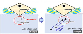 |
| Schematic illustration of how light affects the nucleation (birth) of dislocations (slippages of crystal planes) and dislocation motion, when the sample is also placed under mechanical loading. The Nagoya University/Technical University of Darmstadt research collaboration has found clear evidence that propagation of dislocations in semiconductors is suppressed by light. The likely cause is interaction between dislocations and electrons and holes excited by the light. CREDIT Atsutomo Nakamura |
Abstract:
Semiconductor materials play an indispensable role in our modern information-oriented society. For reliable performance of semiconductor devices, these materials need to have superior mechanical properties: they must be strong as well as resistant to fracture, despite being rich in nanoscale structures.
Light in concert with force reveals how materials become harder when illuminated: When indented by a probe in darkness, wafers of some semiconductors are putty-like. When illuminated by light whose wavelength matches the band gap, they become hard, as electrons and holes freed by
Nagoya, Japan | Posted on March 5th, 2021Recently, it has become increasingly clear that the optical environment affects the structural strength of semiconductor materials. The effect can be much more significant than expected, especially in light-sensitive semiconductors, and particularly since due to technological constraints or fabrication cost many semiconductors can only be mass-produced in very small and thin sizes. Moreover, laboratory testing of their strength has generally been performed on large samples. In the light of the recent explosion in emerging nanoscale applications, all of this suggests that there is an urgent need for the strength of semiconductor materials to be reappraised under controlled illumination conditions and thin sample sizes.
To this end, Professor Atsutomo Nakamura's group at Nagoya University, Japan, and Dr. Xufei Fang's group at the Technical University of Darmstadt have developed a technique for quantitatively studying the effect of light on nanoscale mechanical properties of thin wafers of semiconductors or any other crystalline material. They call it a "photoindentation" method. Essentially, a tiny, pointy probe indents the material while it is illuminated by light under controlled conditions, and the depth and rate at which the probe indents the surface can be measured. The probe creates dislocations - slippages of crystal planes - near the surface, and using a transmission electron microscope the researchers observe the effect of light at a range of wavelengths on dislocation nucleation (the birth of new dislocations) and dislocation mobility (the dislocations' gliding or sliding away from the point where they were created). The nucleation and mobility are measured separately for the first time and is one of the novelties of the photoindentation technique.
The researchers have discovered that while light has a marginal effect on the generation of dislocations under mechanical loading, it has a much stronger effect on the motion of dislocations. When a dislocation occurs, it is energetically favorable for it to expand and join up (nucleate) with others, and the imperfection gets bigger. Illumination by light does not affect this: the electrons and holes excited in the semiconductor by the light (the "photo-excited carriers") do not affect the strain energy of the dislocation, and it is this energy that determines the "line tension" of the dislocation that controls the nucleation process.
On the other hand, dislocations can also move in a so-called "glide motion", during which photo-excited carriers are dragged by dislocations via electrostatic interaction. The effect of photo-excited carriers on this dislocation motion is much more pronounced: if enough carriers are produced, the material becomes much stronger.
This effect is strikingly demonstrated when the same experiment is carried out in complete darkness and then under illumination with light at a wavelength that matches the semiconductor band gap (which produces an increased number of photo-excited carriers). When indented, any solid material initially undergoes "plastic deformation" - changing shape without springing back, somewhat like putty - until the load becomes too great, upon which it cracks. The Nagoya University research group demonstrated that the inorganic semiconductor zinc sulfide (ZnS) in total darkness behaves somewhat like putty, deforming by a huge 45% under shear strain without cracking or falling apart. However, when illuminated at the correct wavelength, it becomes quite hard. At other wavelengths it becomes not quite as hard.
The new findings demonstrate that purely plastic deformation without crack formation in semiconductor materials occurs at the nanoscale. With regards to mechanical behaviour, these semiconductors therefore resemble metallic materials. This newly established, robust experimental protocol makes it possible to evaluate the effect of light on the strength of even non-semiconducting materials that are very thin. Professor Nakamura notes: "One particularly important aspect is that non-semiconductors can exhibit semiconducting properties near the surface, due to oxidation, for instance, and since the starting point of deformation or fracture is often the surface, it is of great significance to establish a method for accurately measuring the strength of materials under controlled illumination conditions at the very surface, on a nanoscale."
The hardening effect that electron-hole pairs freed by light illumination have on material strength - by suppressing the propagation of dislocations, particularly near the surface - is part of a paradigm shift in the science of material strength. Conventionally, when considering the strength of a material, the atomic arrangement was the smallest unit. In other words, there was a premise that the strength of the material could be understood from the atomic arrangement and elasticity theory. However, recent studies have reported that the strength characteristics of materials change significantly due to external influences such as light and an electric field. Therefore, Professor Nakamura notes, "it is becoming more and more accepted that other viewpoints must be added to the theory of material strength which include the motion of electrons and holes that are smaller than atoms."
"This study reaffirms the quantum-level effect on the strength of such materials. In this respect, it can be said that this research has achieved one milestone in the paradigm shift in the field of material strength that is currently occurring."
Dr. Xufei Fang adds: "Now that the creation of devices on the true nanoscale is becoming a reality, the impact of light on the structural strength of various inorganic semiconductors is an issue to be considered."
###
Funding information: This study was mainly supported by JST PRESTO (Grant Number JPMJPR199A). A part of this study was financially supported by JSPS KAKENHI (Grant Numbers JP17H06094, JP18H03840, JP19H05786, JP19K22050) and Athene Young Investigator Programme from TU Darmstadt, Germany.
####
For more information, please click here
Contacts:
Professor Atsutomo Nakamura
@NagoyaUniv
Copyright © Nagoya University
If you have a comment, please Contact us.Issuers of news releases, not 7th Wave, Inc. or Nanotechnology Now, are solely responsible for the accuracy of the content.
Bookmark:


| Related Links |
| Related News Press |
News and information
![]() Quantum computer improves AI predictions April 17th, 2026
Quantum computer improves AI predictions April 17th, 2026
![]() Flexible sensor gains sensitivity under pressure April 17th, 2026
Flexible sensor gains sensitivity under pressure April 17th, 2026
![]() A reusable chip for particulate matter sensing April 17th, 2026
A reusable chip for particulate matter sensing April 17th, 2026
![]() Detecting vibrational quantum beating in the predissociation dynamics of SF6 using time-resolved photoelectron spectroscopy April 17th, 2026
Detecting vibrational quantum beating in the predissociation dynamics of SF6 using time-resolved photoelectron spectroscopy April 17th, 2026
Possible Futures
![]() A fundamentally new therapeutic approach to cystic fibrosis: Nanobody repairs cellular defect April 17th, 2026
A fundamentally new therapeutic approach to cystic fibrosis: Nanobody repairs cellular defect April 17th, 2026
![]() UC Irvine physicists discover method to reverse �quantum scrambling� : The work addresses the problem of information loss in quantum computing system April 17th, 2026
UC Irvine physicists discover method to reverse �quantum scrambling� : The work addresses the problem of information loss in quantum computing system April 17th, 2026
Chip Technology
![]() A reusable chip for particulate matter sensing April 17th, 2026
A reusable chip for particulate matter sensing April 17th, 2026
![]() Metasurfaces smooth light to boost magnetic sensing precision January 30th, 2026
Metasurfaces smooth light to boost magnetic sensing precision January 30th, 2026
Discoveries
![]() Quantum computer improves AI predictions April 17th, 2026
Quantum computer improves AI predictions April 17th, 2026
![]() Flexible sensor gains sensitivity under pressure April 17th, 2026
Flexible sensor gains sensitivity under pressure April 17th, 2026
![]() A reusable chip for particulate matter sensing April 17th, 2026
A reusable chip for particulate matter sensing April 17th, 2026
![]() Detecting vibrational quantum beating in the predissociation dynamics of SF6 using time-resolved photoelectron spectroscopy April 17th, 2026
Detecting vibrational quantum beating in the predissociation dynamics of SF6 using time-resolved photoelectron spectroscopy April 17th, 2026
Materials/Metamaterials/Magnetoresistance
![]() First real-time observation of two-dimensional melting process: Researchers at Mainz University unveil new insights into magnetic vortex structures August 8th, 2025
First real-time observation of two-dimensional melting process: Researchers at Mainz University unveil new insights into magnetic vortex structures August 8th, 2025
![]() Researchers unveil a groundbreaking clay-based solution to capture carbon dioxide and combat climate change June 6th, 2025
Researchers unveil a groundbreaking clay-based solution to capture carbon dioxide and combat climate change June 6th, 2025
![]() A 1960s idea inspires NBI researchers to study hitherto inaccessible quantum states June 6th, 2025
A 1960s idea inspires NBI researchers to study hitherto inaccessible quantum states June 6th, 2025
![]() Institute for Nanoscience hosts annual proposal planning meeting May 16th, 2025
Institute for Nanoscience hosts annual proposal planning meeting May 16th, 2025
Announcements
![]() A fundamentally new therapeutic approach to cystic fibrosis: Nanobody repairs cellular defect April 17th, 2026
A fundamentally new therapeutic approach to cystic fibrosis: Nanobody repairs cellular defect April 17th, 2026
![]() UC Irvine physicists discover method to reverse �quantum scrambling� : The work addresses the problem of information loss in quantum computing system April 17th, 2026
UC Irvine physicists discover method to reverse �quantum scrambling� : The work addresses the problem of information loss in quantum computing system April 17th, 2026
Interviews/Book Reviews/Essays/Reports/Podcasts/Journals/White papers/Posters
![]() A fundamentally new therapeutic approach to cystic fibrosis: Nanobody repairs cellular defect April 17th, 2026
A fundamentally new therapeutic approach to cystic fibrosis: Nanobody repairs cellular defect April 17th, 2026
![]() UC Irvine physicists discover method to reverse �quantum scrambling� : The work addresses the problem of information loss in quantum computing system April 17th, 2026
UC Irvine physicists discover method to reverse �quantum scrambling� : The work addresses the problem of information loss in quantum computing system April 17th, 2026
Photonics/Optics/Lasers
![]() Metasurfaces smooth light to boost magnetic sensing precision January 30th, 2026
Metasurfaces smooth light to boost magnetic sensing precision January 30th, 2026
![]() From sensors to smart systems: the rise of AI-driven photonic noses January 30th, 2026
From sensors to smart systems: the rise of AI-driven photonic noses January 30th, 2026
|
|
||
|
|
||
| The latest news from around the world, FREE | ||
|
|
||
|
|
||
| Premium Products | ||
|
|
||
|
Only the news you want to read!
Learn More |
||
|
|
||
|
Full-service, expert consulting
Learn More |
||
|
|
||