Home > Press > New way to control electrical charge in 2D materials: Put a flake on it
 |
| Physicists at Washington University in St. Louis have discovered how to locally add electrical charge to an atomically thin graphene device by layering flakes of another thin material, alpha-RuCl3, on top of it. Here, a layered device transfers electric charge. CREDIT (Image courtesy Nano Letters) |
Abstract:
Physicists at Washington University in St. Louis have discovered how to locally add electrical charge to an atomically thin graphene device by layering flakes of another thin material, alpha-RuCl3, on top of it.
New way to control electrical charge in 2D materials: Put a flake on it
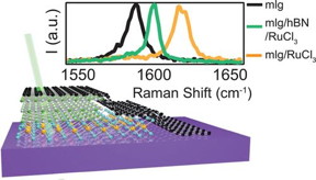
St. Louis, MO | Posted on January 15th, 2021A paper published in the journal Nano Letters describes the charge transfer process in detail. Gaining control of the flow of electrical current through atomically thin materials is important to potential future applications in photovoltaics or computing.
"In my field, where we study van der Waals heterostructures made by custom-stacking atomically thin materials together, we typically control charge by applying electric fields to the devices," said Erik Henriksen, assistant professor of physics in Arts & Sciences and corresponding author of the new study, along with Ken Burch at Boston College. "But here it now appears we can just add layers of RuCl33. It soaks up a fixed amount of electrons, allowing us to make 'permanent' charge transfers that don't require the external electric field."
Jesse Balgley, a graduate student in Henriksen's laboratory at Washington University, is second author of the study. Li Yang, professor of physics, and his graduate student Xiaobo Lu, also both at Washington University, helped with computational work and calculations, and are also co-authors.
Physicists who study condensed matter are intrigued by alpha-RuCl3 because they would like to exploit certain of its antiferromagnetic properties for quantum spin liquids.
In this new study, the scientists report that alpha-RuCl3 is able to transfer charge to several different types of materials -- not just graphene, Henriksen's personal favorite.
They also found that they only needed to place a single layer of alpha-RuCl3 on top of their devices to create and transfer charge. The process still works, even if the scientists slip a thin sheet of an electrically insulating material between the RuCl3 and the graphene.
"We can control how much charge flows in by varying the thickness of the insulator," Henriksen said. "Also, we are able to physically and spatially separate the source of charge from where it goes -- this is called modulation doping."
Adding charge to a quantum spin liquid is one mechanism thought to underlie the physics of high-temperature superconductivity.
"Anytime you do this, it could get exciting," Henriksen said. "And usually you have to add atoms to bulk materials, which causes lots of disorder. But here, the charge flows right in, no need to change the chemical structure, so it's a 'clean' way to add charge."
####
For more information, please click here
Contacts:
Talia Ogliore
314-935-2919
@WUSTLnews
Copyright © Washington University in St. Louis
If you have a comment, please Contact us.Issuers of news releases, not 7th Wave, Inc. or Nanotechnology Now, are solely responsible for the accuracy of the content.
Bookmark:


| Related Links |
![]() Read more in Nano Letters: Modulation Doping via a Two-Dimensional Atomic Crystalline Acceptor:
Read more in Nano Letters: Modulation Doping via a Two-Dimensional Atomic Crystalline Acceptor:
| Related News Press |
News and information
![]() Quantum computer improves AI predictions April 17th, 2026
Quantum computer improves AI predictions April 17th, 2026
![]() Flexible sensor gains sensitivity under pressure April 17th, 2026
Flexible sensor gains sensitivity under pressure April 17th, 2026
![]() A reusable chip for particulate matter sensing April 17th, 2026
A reusable chip for particulate matter sensing April 17th, 2026
![]() Detecting vibrational quantum beating in the predissociation dynamics of SF6 using time-resolved photoelectron spectroscopy April 17th, 2026
Detecting vibrational quantum beating in the predissociation dynamics of SF6 using time-resolved photoelectron spectroscopy April 17th, 2026
2 Dimensional Materials
![]() Flexible sensor gains sensitivity under pressure April 17th, 2026
Flexible sensor gains sensitivity under pressure April 17th, 2026
Graphene/ Graphite
![]() Electrifying results shed light on graphene foam as a potential material for lab grown cartilage June 6th, 2025
Electrifying results shed light on graphene foam as a potential material for lab grown cartilage June 6th, 2025
![]() Breakthrough in proton barrier films using pore-free graphene oxide: Kumamoto University researchers achieve new milestone in advanced coating technologies September 13th, 2024
Breakthrough in proton barrier films using pore-free graphene oxide: Kumamoto University researchers achieve new milestone in advanced coating technologies September 13th, 2024
Possible Futures
![]() A fundamentally new therapeutic approach to cystic fibrosis: Nanobody repairs cellular defect April 17th, 2026
A fundamentally new therapeutic approach to cystic fibrosis: Nanobody repairs cellular defect April 17th, 2026
![]() UC Irvine physicists discover method to reverse �quantum scrambling� : The work addresses the problem of information loss in quantum computing system April 17th, 2026
UC Irvine physicists discover method to reverse �quantum scrambling� : The work addresses the problem of information loss in quantum computing system April 17th, 2026
Chip Technology
![]() A reusable chip for particulate matter sensing April 17th, 2026
A reusable chip for particulate matter sensing April 17th, 2026
![]() Metasurfaces smooth light to boost magnetic sensing precision January 30th, 2026
Metasurfaces smooth light to boost magnetic sensing precision January 30th, 2026
Discoveries
![]() Quantum computer improves AI predictions April 17th, 2026
Quantum computer improves AI predictions April 17th, 2026
![]() Flexible sensor gains sensitivity under pressure April 17th, 2026
Flexible sensor gains sensitivity under pressure April 17th, 2026
![]() A reusable chip for particulate matter sensing April 17th, 2026
A reusable chip for particulate matter sensing April 17th, 2026
![]() Detecting vibrational quantum beating in the predissociation dynamics of SF6 using time-resolved photoelectron spectroscopy April 17th, 2026
Detecting vibrational quantum beating in the predissociation dynamics of SF6 using time-resolved photoelectron spectroscopy April 17th, 2026
Announcements
![]() A fundamentally new therapeutic approach to cystic fibrosis: Nanobody repairs cellular defect April 17th, 2026
A fundamentally new therapeutic approach to cystic fibrosis: Nanobody repairs cellular defect April 17th, 2026
![]() UC Irvine physicists discover method to reverse �quantum scrambling� : The work addresses the problem of information loss in quantum computing system April 17th, 2026
UC Irvine physicists discover method to reverse �quantum scrambling� : The work addresses the problem of information loss in quantum computing system April 17th, 2026
Interviews/Book Reviews/Essays/Reports/Podcasts/Journals/White papers/Posters
![]() A fundamentally new therapeutic approach to cystic fibrosis: Nanobody repairs cellular defect April 17th, 2026
A fundamentally new therapeutic approach to cystic fibrosis: Nanobody repairs cellular defect April 17th, 2026
![]() UC Irvine physicists discover method to reverse �quantum scrambling� : The work addresses the problem of information loss in quantum computing system April 17th, 2026
UC Irvine physicists discover method to reverse �quantum scrambling� : The work addresses the problem of information loss in quantum computing system April 17th, 2026
|
|
||
|
|
||
| The latest news from around the world, FREE | ||
|
|
||
|
|
||
| Premium Products | ||
|
|
||
|
Only the news you want to read!
Learn More |
||
|
|
||
|
Full-service, expert consulting
Learn More |
||
|
|
||