Home > Press > Configurable circuit technology poised to expand silicon photonic applications: Chips can be programmed after fabrication for use in communication, computing or biomedical applications
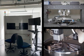 |
| The researchers have developed a wafer-scale prober that is being tested at the University of Southampton (left). The prober can autonomously and accurately perform optical and electrical device testing along with laser annealing at an average speed of less than 30 seconds per device. Images on the right show a closer look at the software driven positioning stage for autonomous measurements (top-right) and the input/output fibers positioned on top of the 8-inch wafer (bottom-right). CREDIT Xia Chen, University of Southampton |
Abstract:
Researchers have developed a new way to build power efficient and programmable integrated switching units on a silicon photonics chip. The new technology is poised to reduce production costs by allowing a generic optical circuit to be fabricated in bulk and then later programmed for specific applications such as communications systems, LIDAR circuits or computing applications.
Configurable circuit technology poised to expand silicon photonic applications: Chips can be programmed after fabrication for use in communication, computing or biomedical applications
Washington, DC | Posted on May 29th, 2020"Silicon photonics is capable of integrating optical devices and advanced microelectronic circuits all on a single chip," said research team member Xia Chen from the University of Southampton. "We expect configurable silicon photonics circuits to greatly expand the scope of applications for silicon photonics while also reducing costs, making this technology more useful for consumer applications."
In The Optical Society (OSA) journal Optics Express, researchers led by Graham Reed demonstrate the new approach in switching units that can be used as building blocks to create larger chip-based, programmable photonic circuits.
"The technology we developed will have a wide range of applications," said Chen. "For example, it could be used to make integrated sensing devices to detect biochemical and medical substances as well as optical transceivers for connections used in high-performance computing systems and data centers."
Erasable components
The new work builds on earlier research in which the investigators developed an erasable version of an optical component known as a grating coupler by implanting germanium ions into silicon. These ions induce damage that changes silicon's refractive index in that area. Heating the local area using a laser annealing process can then be used to reverse the refractive index and erase the grating coupler.
In the Optics Express paper, the researchers describe how they applied the same germanium ion implantation technique to create erasable waveguides and directional couplers, components that can be used to make reconfigurable circuits and switches. This represents the first time that sub-micron erasable waveguides have been created in silicon.
"We normally think about ion implantation as something that will induce large optical losses in a photonic integrated circuit," said Chen. "However, we found that a carefully designed structure and using the right ion implantation recipe can create a waveguide that carries optical signals with reasonable optical loss."
Building programmable circuits
They demonstrated the new approach by designing and fabricating waveguides, directional couplers and 1 X 4 and 2 X 2 switching circuits, using the University of Southampton's Cornerstone fabrication foundry. Photonic devices from different chips tested both before and after programming with laser annealing showed consistent performance.
Because the technique involves physically changing the routing of the photonic waveguide via a one-time operation, no additional power is needed to retain the configuration when programmed. The researchers have also discovered that electrical annealing, using a local integrated heater, as well as laser annealing can be used to program the circuits.
The researchers are working with a company called ficonTEC to make this technology practical outside the laboratory by developing a way to apply the laser and/or electrical annealing process at wafer scale, using a conventional wafer prober (wafer testing machine), so that hundreds or thousands of chips could be programmed automatically. They are currently working on integrating the laser and electrical annealing processes into such a wafer-scale prober -- an instrument found in most electronic-photonic foundries -- being testing at the University of Southampton.
###
This research is part of a project funded by the Engineering and Physical Sciences Research Council to transform silicon photonics and bring it to mass markets.
####
About The Optical Society
Founded in 1916, The Optical Society (OSA) is the leading professional organization for scientists, engineers, students and business leaders who fuel discoveries, shape real-life applications and accelerate achievements in the science of light. Through world-renowned publications, meetings and membership initiatives, OSA provides quality research, inspired interactions and dedicated resources for its extensive global network of optics and photonics experts. For more information, visit osa.org.
Media Contact:
About Optics Express
Optics Express reports on scientific and technology innovations in all aspects of optics and photonics. The bi-weekly journal provides rapid publication of original, peer-reviewed papers. It is published by The Optical Society (OSA) and led by Editor-in-Chief James Leger of the University of Minnesota, USA. Optics Express is an open-access journal and is available at no cost to readers online at OSA Publishing.
For more information, please click here
Contacts:
James Merrick
410-262-9407
@opticalsociety
Copyright © The Optical Society
If you have a comment, please Contact us.Issuers of news releases, not 7th Wave, Inc. or Nanotechnology Now, are solely responsible for the accuracy of the content.
Bookmark:


| Related Links |
| Related News Press |
News and information
![]() Decoding hydrogen‑bond network of electrolyte for cryogenic durable aqueous zinc‑ion batteries January 30th, 2026
Decoding hydrogen‑bond network of electrolyte for cryogenic durable aqueous zinc‑ion batteries January 30th, 2026
![]() COF scaffold membrane with gate‑lane nanostructure for efficient Li+/Mg2+ separation January 30th, 2026
COF scaffold membrane with gate‑lane nanostructure for efficient Li+/Mg2+ separation January 30th, 2026
Possible Futures
![]() Decoding hydrogen‑bond network of electrolyte for cryogenic durable aqueous zinc‑ion batteries January 30th, 2026
Decoding hydrogen‑bond network of electrolyte for cryogenic durable aqueous zinc‑ion batteries January 30th, 2026
![]() COF scaffold membrane with gate‑lane nanostructure for efficient Li+/Mg2+ separation January 30th, 2026
COF scaffold membrane with gate‑lane nanostructure for efficient Li+/Mg2+ separation January 30th, 2026
Chip Technology
![]() Metasurfaces smooth light to boost magnetic sensing precision January 30th, 2026
Metasurfaces smooth light to boost magnetic sensing precision January 30th, 2026
![]() Beyond silicon: Electronics at the scale of a single molecule January 30th, 2026
Beyond silicon: Electronics at the scale of a single molecule January 30th, 2026
![]() Lab to industry: InSe wafer-scale breakthrough for future electronics August 8th, 2025
Lab to industry: InSe wafer-scale breakthrough for future electronics August 8th, 2025
Optical computing/Photonic computing
![]() ICFO researchers overcome long-standing bottleneck in single photon detection with twisted 2D materials August 8th, 2025
ICFO researchers overcome long-standing bottleneck in single photon detection with twisted 2D materials August 8th, 2025
![]() Programmable electron-induced color router array May 14th, 2025
Programmable electron-induced color router array May 14th, 2025
![]() Nanophotonic platform boosts efficiency of nonlinear-optical quantum teleportation April 25th, 2025
Nanophotonic platform boosts efficiency of nonlinear-optical quantum teleportation April 25th, 2025
![]() Groundbreaking research unveils unified theory for optical singularities in photonic microstructures December 13th, 2024
Groundbreaking research unveils unified theory for optical singularities in photonic microstructures December 13th, 2024
Discoveries
![]() From sensors to smart systems: the rise of AI-driven photonic noses January 30th, 2026
From sensors to smart systems: the rise of AI-driven photonic noses January 30th, 2026
![]() Decoding hydrogen‑bond network of electrolyte for cryogenic durable aqueous zinc‑ion batteries January 30th, 2026
Decoding hydrogen‑bond network of electrolyte for cryogenic durable aqueous zinc‑ion batteries January 30th, 2026
![]() COF scaffold membrane with gate‑lane nanostructure for efficient Li+/Mg2+ separation January 30th, 2026
COF scaffold membrane with gate‑lane nanostructure for efficient Li+/Mg2+ separation January 30th, 2026
Announcements
![]() Decoding hydrogen‑bond network of electrolyte for cryogenic durable aqueous zinc‑ion batteries January 30th, 2026
Decoding hydrogen‑bond network of electrolyte for cryogenic durable aqueous zinc‑ion batteries January 30th, 2026
![]() COF scaffold membrane with gate‑lane nanostructure for efficient Li+/Mg2+ separation January 30th, 2026
COF scaffold membrane with gate‑lane nanostructure for efficient Li+/Mg2+ separation January 30th, 2026
Interviews/Book Reviews/Essays/Reports/Podcasts/Journals/White papers/Posters
![]() Metasurfaces smooth light to boost magnetic sensing precision January 30th, 2026
Metasurfaces smooth light to boost magnetic sensing precision January 30th, 2026
![]() COF scaffold membrane with gate‑lane nanostructure for efficient Li+/Mg2+ separation January 30th, 2026
COF scaffold membrane with gate‑lane nanostructure for efficient Li+/Mg2+ separation January 30th, 2026
Photonics/Optics/Lasers
![]() Metasurfaces smooth light to boost magnetic sensing precision January 30th, 2026
Metasurfaces smooth light to boost magnetic sensing precision January 30th, 2026
![]() From sensors to smart systems: the rise of AI-driven photonic noses January 30th, 2026
From sensors to smart systems: the rise of AI-driven photonic noses January 30th, 2026
![]() ICFO researchers overcome long-standing bottleneck in single photon detection with twisted 2D materials August 8th, 2025
ICFO researchers overcome long-standing bottleneck in single photon detection with twisted 2D materials August 8th, 2025
|
|
||
|
|
||
| The latest news from around the world, FREE | ||
|
|
||
|
|
||
| Premium Products | ||
|
|
||
|
Only the news you want to read!
Learn More |
||
|
|
||
|
Full-service, expert consulting
Learn More |
||
|
|
||