Home > Press > Using artificial intelligence to engineer materials' properties: New system of 'strain engineering' can change a material's optical, electrical, and thermal properties
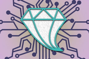 |
| Introducing a small amount of strain into crystalline materials, such as diamond or silicon, can produce significant changes in their properties, researchers have found. The mechanical strain is represented here as a deformation in the diamond's shape. Image: Chelsea Turner, MIT |
Abstract:
Applying just a bit of strain to a piece of semiconductor or other crystalline material can deform the orderly arrangement of atoms in its structure enough to cause dramatic changes in its properties, such as the way it conducts electricity, transmits light, or conducts heat.
Using artificial intelligence to engineer materials' properties: New system of 'strain engineering' can change a material's optical, electrical, and thermal properties
Cambridge, MA | Posted on February 11th, 2019Now, a team of researchers at MIT and in Russia and Singapore have found ways to use artificial intelligence to help predict and control these changes, potentially opening up new avenues of research on advanced materials for future high-tech devices.
The findings appear this week in the Proceedings of the National Academy of Sciences, in a paper authored by MIT professor of nuclear science and engineering and of materials science and engineering Ju Li, MIT Principal Research Scientist Ming Dao, and MIT graduate student Zhe Shi, with Evgeni Tsymbalov and Alexander Shapeev at the Skolkovo Institute of Science and Technology in Russia, and Subra Suresh, the Vannevar Bush Professor Emeritus and former dean of engineering at MIT and current president of Nanyang Technological University in Singapore.
Already, based on earlier work at MIT, some degree of elastic strain has been incorporated in some silicon processor chips. Even a 1 percent change in the structure can in some cases improve the speed of the device by 50 percent, by allowing electrons to move through the material faster.
Recent research by Suresh, Dao, and Yang Lu, a former MIT postdoc now at City University of Hong Kong, showed that even diamond, the strongest and hardest material found in nature, can be elastically stretched by as much as 9 percent without failure when it is in the form of nanometer-sized needles. Li and Yang similarly demonstrated that nanoscale wires of silicon can be stretched purely elastically by more than 15 percent. These discoveries have opened up new avenues to explore how devices can be fabricated with even more dramatic changes in the materials' properties.
Strain made to order
Unlike other ways of changing a material's properties, such as chemical doping, which produce a permanent, static change, strain engineering allows properties to be changed on the fly. "Strain is something you can turn on and off dynamically," Li says.
But the potential of strain-engineered materials has been hampered by the daunting range of possibilities. Strain can be applied in any of six different ways (in three different dimensions, each one of which can produce strain in-and-out or sideways), and with nearly infinite gradations of degree, so the full range of possibilities is impractical to explore simply by trial and error. "It quickly grows to 100 million calculations if we want to map out the entire elastic strain space," Li says.
That's where this team's novel application of machine learning methods comes to the rescue, providing a systematic way of exploring the possibilities and homing in on the appropriate amount and direction of strain to achieve a given set of properties for a particular purpose. "Now we have this very high-accuracy method" that drastically reduces the complexity of the calculations needed, Li says.
"This work is an illustration of how recent advances in seemingly distant fields such as material physics, artificial intelligence, computing, and machine learning can be brought together to advance scientific knowledge that has strong implications for industry application," Suresh says.
The new method, the researchers say, could open up possibilities for creating materials tuned precisely for electronic, optoelectronic, and photonic devices that could find uses for communications, information processing, and energy applications.
The team studied the effects of strain on the bandgap, a key electronic property of semiconductors, in both silicon and diamond. Using their neural network algorithm, they were able to predict with high accuracy how different amounts and orientations of strain would affect the bandgap.
"Tuning" of a bandgap can be a key tool for improving the efficiency of a device, such as a silicon solar cell, by getting it to match more precisely the kind of energy source that it is designed to harness. By fine-tuning its bandgap, for example, it may be possible to make a silicon solar cell that is just as effective at capturing sunlight as its counterparts but is only one-thousandth as thick. In theory, the material "can even change from a semiconductor to a metal, and that would have many applications, if that's doable in a mass-produced product," Li says.
While it's possible in some cases to induce similar changes by other means, such as putting the material in a strong electric field or chemically altering it, those changes tend to have many side effects on the material's behavior, whereas changing the strain has fewer such side effects. For example, Li explains, an electrostatic field often interferes with the operation of the device because it affects the way electricity flows through it. Changing the strain produces no such interference.
Diamond's potential
Diamond has great potential as a semiconductor material, though it's still in its infancy compared to silicon technology. "It's an extreme material, with high carrier mobility," Li says, referring to the way negative and positive carriers of electric current move freely through diamond. Because of that, diamond could be ideal for some kinds of high-frequency electronic devices and for power electronics.
By some measures, Li says, diamond could potentially perform 100,000 times better than silicon. But it has other limitations, including the fact that nobody has yet figured out a good and scalable way to put diamond layers on a large substrate. The material is also difficult to "dope," or introduce other atoms into, a key part of semiconductor manufacturing.
By mounting the material in a frame that can be adjusted to change the amount and orientation of the strain, Dao says, "we can have considerable flexibility" in altering its dopant behavior.
Whereas this study focused specifically on the effects of strain on the materials' bandgap, "the method is generalizable" to other aspects, which affect not only electronic properties but also other properties such as photonic and magnetic behavior, Li says. From the 1 percent strain now being used in commercial chips, many new applications open up now that this team has shown that strains of nearly 10 percent are possible without fracturing. "When you get to more than 7 percent strain, you really change a lot in the material," he says.
"This new method could potentially lead to the design of unprecedented material properties," Li says. "But much further work will be needed to figure out how to impose the strain and how to scale up the process to do it on 100 million transistors on a chip [and ensure that] none of them can fail."
###
The work was supported by the MIT-Skoltech program and Nanyang Technological University.
####
For more information, please click here
Contacts:
Abby Abazorius
617-253-2709
Copyright © Massachusetts Institute of Technology
If you have a comment, please Contact us.Issuers of news releases, not 7th Wave, Inc. or Nanotechnology Now, are solely responsible for the accuracy of the content.
Bookmark:


| Related Links |
![]() Paper: �Deep elastic strain engineering of bandgap through machine learning.�:
Paper: �Deep elastic strain engineering of bandgap through machine learning.�:
| Related News Press |
News and information
![]() Quantum computer improves AI predictions April 17th, 2026
Quantum computer improves AI predictions April 17th, 2026
![]() Flexible sensor gains sensitivity under pressure April 17th, 2026
Flexible sensor gains sensitivity under pressure April 17th, 2026
![]() A reusable chip for particulate matter sensing April 17th, 2026
A reusable chip for particulate matter sensing April 17th, 2026
![]() Detecting vibrational quantum beating in the predissociation dynamics of SF6 using time-resolved photoelectron spectroscopy April 17th, 2026
Detecting vibrational quantum beating in the predissociation dynamics of SF6 using time-resolved photoelectron spectroscopy April 17th, 2026
Possible Futures
![]() A fundamentally new therapeutic approach to cystic fibrosis: Nanobody repairs cellular defect April 17th, 2026
A fundamentally new therapeutic approach to cystic fibrosis: Nanobody repairs cellular defect April 17th, 2026
![]() UC Irvine physicists discover method to reverse �quantum scrambling� : The work addresses the problem of information loss in quantum computing system April 17th, 2026
UC Irvine physicists discover method to reverse �quantum scrambling� : The work addresses the problem of information loss in quantum computing system April 17th, 2026
Chip Technology
![]() A reusable chip for particulate matter sensing April 17th, 2026
A reusable chip for particulate matter sensing April 17th, 2026
![]() Metasurfaces smooth light to boost magnetic sensing precision January 30th, 2026
Metasurfaces smooth light to boost magnetic sensing precision January 30th, 2026
Materials/Metamaterials/Magnetoresistance
![]() First real-time observation of two-dimensional melting process: Researchers at Mainz University unveil new insights into magnetic vortex structures August 8th, 2025
First real-time observation of two-dimensional melting process: Researchers at Mainz University unveil new insights into magnetic vortex structures August 8th, 2025
![]() Researchers unveil a groundbreaking clay-based solution to capture carbon dioxide and combat climate change June 6th, 2025
Researchers unveil a groundbreaking clay-based solution to capture carbon dioxide and combat climate change June 6th, 2025
![]() A 1960s idea inspires NBI researchers to study hitherto inaccessible quantum states June 6th, 2025
A 1960s idea inspires NBI researchers to study hitherto inaccessible quantum states June 6th, 2025
![]() Institute for Nanoscience hosts annual proposal planning meeting May 16th, 2025
Institute for Nanoscience hosts annual proposal planning meeting May 16th, 2025
Announcements
![]() A fundamentally new therapeutic approach to cystic fibrosis: Nanobody repairs cellular defect April 17th, 2026
A fundamentally new therapeutic approach to cystic fibrosis: Nanobody repairs cellular defect April 17th, 2026
![]() UC Irvine physicists discover method to reverse �quantum scrambling� : The work addresses the problem of information loss in quantum computing system April 17th, 2026
UC Irvine physicists discover method to reverse �quantum scrambling� : The work addresses the problem of information loss in quantum computing system April 17th, 2026
Interviews/Book Reviews/Essays/Reports/Podcasts/Journals/White papers/Posters
![]() A fundamentally new therapeutic approach to cystic fibrosis: Nanobody repairs cellular defect April 17th, 2026
A fundamentally new therapeutic approach to cystic fibrosis: Nanobody repairs cellular defect April 17th, 2026
![]() UC Irvine physicists discover method to reverse �quantum scrambling� : The work addresses the problem of information loss in quantum computing system April 17th, 2026
UC Irvine physicists discover method to reverse �quantum scrambling� : The work addresses the problem of information loss in quantum computing system April 17th, 2026
Artificial Intelligence
![]() Quantum computer improves AI predictions April 17th, 2026
Quantum computer improves AI predictions April 17th, 2026
![]() From sensors to smart systems: the rise of AI-driven photonic noses January 30th, 2026
From sensors to smart systems: the rise of AI-driven photonic noses January 30th, 2026
![]() New quantum encoding methods slash circuit complexity in machine learning November 8th, 2024
New quantum encoding methods slash circuit complexity in machine learning November 8th, 2024
Research partnerships
![]() Lab to industry: InSe wafer-scale breakthrough for future electronics August 8th, 2025
Lab to industry: InSe wafer-scale breakthrough for future electronics August 8th, 2025
![]() HKU physicists uncover hidden order in the quantum world through deconfined quantum critical points April 25th, 2025
HKU physicists uncover hidden order in the quantum world through deconfined quantum critical points April 25th, 2025
|
|
||
|
|
||
| The latest news from around the world, FREE | ||
|
|
||
|
|
||
| Premium Products | ||
|
|
||
|
Only the news you want to read!
Learn More |
||
|
|
||
|
Full-service, expert consulting
Learn More |
||
|
|
||