Home > Press > Nanoscribe Presents Successor Model Photonic Professional GT2 for High-Resolution 3D Microfabrication: The first ever production of structures in millimeter size with micrometer precision
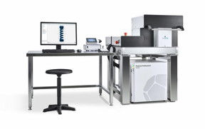 |
| Img 1: The new Photonic Professional GT2 3D printer enables the production of larger structures with higher precision in shorter times. Img 2: Filigree structures up to the millimeter range can be printed with the highest resolution. |
Abstract:
With the successor model Photonic Professional GT2, Nanoscribe, the world's leading manufacturer of 3D printers for microfabrication, offers new solutions for additive manufacturing and maskless lithography. Thanks to optimized hardware and software components as well as IP-Q printing material especially developed for larger volumes, high-resolution microstructures up to a height of 8 mm can now be produced for the first time. While Nanoscribe devices have always been optimally suited to the additive production of the finest structures, objects with submicrometer details from typically 160 nanometers up to the millimeter range on a printing area of up to 100x100 mm˛ can now be produced in a very short time.
Nanoscribe Presents Successor Model Photonic Professional GT2 for High-Resolution 3D Microfabrication: The first ever production of structures in millimeter size with micrometer precision
Eggenstein-Leopoldshafen, Germany | Posted on December 4th, 2018
Depending on the desired size and resolution, users can choose from sets of objectives, substrates, materials, and automated processes tailored to their applications. The user-friendly 3D printing workflow enables the fabrication of individual elements with maximum shape accuracy and surface smoothness, meeting the requirements for microlenses in the smartphone industry or filigree scaffold structures in cell biology. Likewise, high-precision masters can be produced for molding processes in series production on a scale and design freedom that can neither be achieved with alternative subtractive nor additive manufacturing technologies.
"The extension of the maximum print volumes toward the macroscale was a great wish of our customers and project partners from industry," says Nanoscribe CEO Martin Hermatschweiler. "With this relaunch of our extremely successful generation of Photonic Professional devices, we have now succeeded in overcoming previous physical limitations and increasing the performance of the devices by a factor of up to 10 in terms of productivity and speed," adds Hermatschweiler.
Extended Range of Applications for Industry
The new Photonic Professional GT2 3D printer can significantly shorten product development cycles, especially in cases where large-volume structures in the millimeter range are required, such as for microfluidic elements (filters or nozzles), lab-on-a-chip applications, or micro rapid prototyping. In the field of sensor and actuator technology, various product components can now be printed quickly and precisely on MEMS components or silicon chips without further adjustment or assembly processes thanks to the variety of printable substrates.
Nanoscribe_PPGT_Sample
Photonic Professional GT2 systems will also open up completely new possibilities in the field of medical technology, such as the direct printing of micro-optics on glass fibers for minimally invasive endoscopes or the manufacture of microneedles for painless drug delivery through the skin.
Functional Principle of Two-Photon Polymerization in 3D Printing
Nanoscribe systems combine the technology of two-photon polymerization with the workflow of a conventional 3D printing process. An ultra-precisely focused femtosecond laser cures a photosensitive material layer-by-layer. In a simple workflow, software especially developed for the printing process supports the import of CAD models with extensive configuration options, including a wide selection of preset parameters. A 3D preview as well as a real-time camera support the user in optimal adjustment and monitoring of the printing process.
The proprietary software programs DeScribe and NanoWrite have been enhanced for the new printer generation. With intelligent printing strategies, up to 10 times higher printing speeds are achieved. Thanks to enormous design freedom, Nanoscribe printers can produce structures of varying complexity: for example, grating-like high resolution photonic structures in 2D, hemispherical microlenses with vertical slopes in 2.5D, and complex 3D objects such as gas-dynamic micronozzles. Parts printed with replicable topographies can also serve as polymer masters for molding processes. Using galvanic processes, 3D printed polymer masters are metallized in order to be used as nickel shims for mass production, for example, in injection molding.
Among 3D printing technologies, two-photon polymerization is best qualified for finest structures on the micro- and mesoscale. While other 3D printing technologies, such as Polyjet, DLP (Digital Light Processing), or SLA (stereolithography), only excel from the centimeter range, the strengths of Photonic Professional GT2 systems lie in the ultra-precise 3D microfabrication.
####
About Nanoscribe
Nanoscribe GmbH, located in Eggenstein-Leopoldshafen near Karlsruhe (Germany), develops and provides 3D printers for microfabrication as well as photoresins and process solutions. Since the foundation in 2007, the company has managed to turn from a spin-off of the Karlsruhe Institute of Technology (KIT, Germany) to a medium-sized company with more than 65 employees. Nanoscribe established itself as a global market- and technology leader for 3D printing on the micro- and mesoscale. Worldwide, more than 1,000 users in top universities and pioneer companies benefit from Nanoscribe´s technology and award-winning solutions for microfabrication.
For more information, please click here
Contacts:
Anke Werner
Media Contact
Phone +49 721 981 980 501
Copyright © Nanoscribe
If you have a comment, please Contact us.Issuers of news releases, not 7th Wave, Inc. or Nanotechnology Now, are solely responsible for the accuracy of the content.
Bookmark:


| Related News Press |
News and information
![]() Simulating magnetization in a Heisenberg quantum spin chain April 5th, 2024
Simulating magnetization in a Heisenberg quantum spin chain April 5th, 2024
![]() NRL charters Navy’s quantum inertial navigation path to reduce drift April 5th, 2024
NRL charters Navy’s quantum inertial navigation path to reduce drift April 5th, 2024
![]() Discovery points path to flash-like memory for storing qubits: Rice find could hasten development of nonvolatile quantum memory April 5th, 2024
Discovery points path to flash-like memory for storing qubits: Rice find could hasten development of nonvolatile quantum memory April 5th, 2024
3D & 4D printing/Additive-manufacturing
![]() Presenting: Ultrasound-based printing of 3D materials—potentially inside the body December 8th, 2023
Presenting: Ultrasound-based printing of 3D materials—potentially inside the body December 8th, 2023
![]() Fiber sensing scientists invent 3D printed fiber microprobe for measuring in vivo biomechanical properties of tissue and even single cell February 10th, 2023
Fiber sensing scientists invent 3D printed fiber microprobe for measuring in vivo biomechanical properties of tissue and even single cell February 10th, 2023
![]() 3D-printed decoder, AI-enabled image compression could enable higher-res displays December 9th, 2022
3D-printed decoder, AI-enabled image compression could enable higher-res displays December 9th, 2022
![]() Researchers design new inks for 3D-printable wearable bioelectronics: Potential uses include printing electronic tattoos for medical tracking applications August 19th, 2022
Researchers design new inks for 3D-printable wearable bioelectronics: Potential uses include printing electronic tattoos for medical tracking applications August 19th, 2022
Chip Technology
![]() Discovery points path to flash-like memory for storing qubits: Rice find could hasten development of nonvolatile quantum memory April 5th, 2024
Discovery points path to flash-like memory for storing qubits: Rice find could hasten development of nonvolatile quantum memory April 5th, 2024
![]() Utilizing palladium for addressing contact issues of buried oxide thin film transistors April 5th, 2024
Utilizing palladium for addressing contact issues of buried oxide thin film transistors April 5th, 2024
![]() HKUST researchers develop new integration technique for efficient coupling of III-V and silicon February 16th, 2024
HKUST researchers develop new integration technique for efficient coupling of III-V and silicon February 16th, 2024
Announcements
![]() NRL charters Navy’s quantum inertial navigation path to reduce drift April 5th, 2024
NRL charters Navy’s quantum inertial navigation path to reduce drift April 5th, 2024
![]() Discovery points path to flash-like memory for storing qubits: Rice find could hasten development of nonvolatile quantum memory April 5th, 2024
Discovery points path to flash-like memory for storing qubits: Rice find could hasten development of nonvolatile quantum memory April 5th, 2024
Tools
![]() Ferroelectrically modulate the Fermi level of graphene oxide to enhance SERS response November 3rd, 2023
Ferroelectrically modulate the Fermi level of graphene oxide to enhance SERS response November 3rd, 2023
![]() The USTC realizes In situ electron paramagnetic resonance spectroscopy using single nanodiamond sensors November 3rd, 2023
The USTC realizes In situ electron paramagnetic resonance spectroscopy using single nanodiamond sensors November 3rd, 2023
Photonics/Optics/Lasers
![]() With VECSELs towards the quantum internet Fraunhofer: IAF achieves record output power with VECSEL for quantum frequency converters April 5th, 2024
With VECSELs towards the quantum internet Fraunhofer: IAF achieves record output power with VECSEL for quantum frequency converters April 5th, 2024
![]() Nanoscale CL thermometry with lanthanide-doped heavy-metal oxide in TEM March 8th, 2024
Nanoscale CL thermometry with lanthanide-doped heavy-metal oxide in TEM March 8th, 2024
![]() Optically trapped quantum droplets of light can bind together to form macroscopic complexes March 8th, 2024
Optically trapped quantum droplets of light can bind together to form macroscopic complexes March 8th, 2024
![]() HKUST researchers develop new integration technique for efficient coupling of III-V and silicon February 16th, 2024
HKUST researchers develop new integration technique for efficient coupling of III-V and silicon February 16th, 2024
Printing/Lithography/Inkjet/Inks/Bio-printing/Dyes
![]() Presenting: Ultrasound-based printing of 3D materials—potentially inside the body December 8th, 2023
Presenting: Ultrasound-based printing of 3D materials—potentially inside the body December 8th, 2023
![]() Simple ballpoint pen can write custom LEDs August 11th, 2023
Simple ballpoint pen can write custom LEDs August 11th, 2023
![]() Disposable electronics on a simple sheet of paper October 7th, 2022
Disposable electronics on a simple sheet of paper October 7th, 2022
|
|
||
|
|
||
| The latest news from around the world, FREE | ||
|
|
||
|
|
||
| Premium Products | ||
|
|
||
|
Only the news you want to read!
Learn More |
||
|
|
||
|
Full-service, expert consulting
Learn More |
||
|
|
||