Home > Press > JPK reports on the use of STM to study surface plasmons in the Molecular Science Group at ISMO – Institut des Sciences Moléculaires d’Orsay
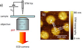 |
| STM plasmonic crystal: Schematic of the experiment and STM image of sample – a gold nanoparticle array (article Optics Express, 4, 26186 (2016)) |
Abstract:
JPK Instruments, a world-leading manufacturer of nanoanalytic instrumentation for research in life sciences and soft matter, reports on how STM is being used to study surface plasmons in the Molecular Nanoscience Group at ISMO – Institut des Sciences Moléculaires d’Orsay – CNRS and the Université Paris-Sud.
JPK reports on the use of STM to study surface plasmons in the Molecular Science Group at ISMO – Institut des Sciences Moléculaires d’Orsay
Berlin, Germany | Posted on February 8th, 2017One of the research goals of the Molecular Nanoscience Group at ISMO is to work towards circuits and devices in which surface plasmons (not electrons or photons) are used to transfer and manipulate information. However, why develop plasmonics when there are already solutions using electronics and photonics? Electronics has been extremely successful in the area of miniaturization, leading to computers which now fit in the palm of your hand. However, electronic devices are fundamentally limited in speed by the generation of heat. On the other hand, the use of photonics has successfully enabled fast data downloads from the Internet since optical fiber connections offer high bandwidth. Optical devices are also limited, this time in terms of size, due to the diffraction limit of light. The goal of this research group is the development of plasmonics which combines the advantages of electronics and photonics, thus producing miniaturized, high bandwidth circuits and devices which use surface plasmons. To bring this to a commercial reality, a local, low energy electrical source of surface plasmon polaritons is required.
For this research program to develop, group leader, Dr Elizabeth Boer-Duchemin takes up the story. “We propose to use an electrically biased tunnel junction as this local electrical plasmon source, and as a prototype, we consider the tunnel junction formed between the tip of a scanning tunneling microscope and a metallic sample. We chose to work with JPK for a number of reasons. First and foremost, the fact that the JPK STM is easily mounted on an inverted optical microscope (for surface plasmon detection) is essential for us. The design of the tip-assisted-optics (TAO) stage makes it easy to move both tip and sample independently. In our experiments, we use the STM to excite surface plasmons. These then radiate as photons which is the emitted light that we finally detect. I would also like to thank the engineering team at JPK who were extremely helpful in the project. This is a very unusual application and they played a vital part in the writing of specialised scripts to enable the work.”
The Group has been very active in publishing papers on this work. In 2016, these included publications such as Nanotechnology,1 and Optics Express2.
For more details about JPK's STM and AFM systems and their applications for the materials & nano sciences, please contact JPK on +49 30726243 500. Alternatively, please visit the web site: www.jpk.com/ or see more on Facebook: www.jpk.com/facebook and on You Tube: www.youtube.com/jpkinstruments.
References
1 “The mechanism of light emission from a scanning tunnelling microscope operating in air”, B. Rogez, S. Cao, G. Dujardin, G. Comtet, E. Le Moal, A. Mayne and E. Boer-Duchemin, Nanotechnology, 27, 465201 (2016).
2 “Surface plasmon polariton beams from an electrically excited plasmonic crystal”, D Canneson, E Le Moal, S Cao, X Quelin, H Dallaporta, G Dujardin & Elizabeth Boer-Duchemin, Optics Express, 4, 26186 (2016)
####
About JPK Instruments
JPK Instruments AG is a world-leading manufacturer of nanoanalytic instruments - particularly atomic force microscope (AFM) systems and optical tweezers - for a broad range of applications reaching from soft matter physics to nano-optics, from surface chemistry to cell and molecular biology. From its earliest days applying atomic force microscope (AFM) technology, JPK has recognized the opportunities provided by nanotechnology for transforming life sciences and soft matter research. This focus has driven JPK's success in uniting the worlds of nanotechnology tools and life science applications by offering cutting-edge technology and unique applications expertise. Headquartered in Berlin and with direct operations in Dresden, Cambridge (UK), Singapore, Tokyo, Shanghai (China), Paris (France) and Carpinteria (USA), JPK maintains a global network of distributors and support centers and provides on the spot applications and service support to an ever-growing community of researchers.
For more information, please click here
Contacts:
JPK Instruments AG
Colditzstrasse 34-36
Haus 13, Eingang B
Berlin 12099
Germany
T +49 30726243 500
F +49 30726243 999
http://www.jpk.com/
Talking Science Limited
39 de Bohun Court
Saffron Walden
Essex CB10 2BA UK
T +44(0)1799 521881
M +44(0)7843 012997
www.talking-science.com.
Copyright © JPK Instruments
If you have a comment, please Contact us.Issuers of news releases, not 7th Wave, Inc. or Nanotechnology Now, are solely responsible for the accuracy of the content.
Bookmark:


| Related News Press |
News and information
![]() Researchers develop molecular qubits that communicate at telecom frequencies October 3rd, 2025
Researchers develop molecular qubits that communicate at telecom frequencies October 3rd, 2025
![]() Next-generation quantum communication October 3rd, 2025
Next-generation quantum communication October 3rd, 2025
![]() "Nanoreactor" cage uses visible light for catalytic and ultra-selective cross-cycloadditions October 3rd, 2025
"Nanoreactor" cage uses visible light for catalytic and ultra-selective cross-cycloadditions October 3rd, 2025
Imaging
![]() ICFO researchers overcome long-standing bottleneck in single photon detection with twisted 2D materials August 8th, 2025
ICFO researchers overcome long-standing bottleneck in single photon detection with twisted 2D materials August 8th, 2025
![]() Simple algorithm paired with standard imaging tool could predict failure in lithium metal batteries August 8th, 2025
Simple algorithm paired with standard imaging tool could predict failure in lithium metal batteries August 8th, 2025
![]() First real-time observation of two-dimensional melting process: Researchers at Mainz University unveil new insights into magnetic vortex structures August 8th, 2025
First real-time observation of two-dimensional melting process: Researchers at Mainz University unveil new insights into magnetic vortex structures August 8th, 2025
![]() New imaging approach transforms study of bacterial biofilms August 8th, 2025
New imaging approach transforms study of bacterial biofilms August 8th, 2025
Discoveries
![]() Researchers develop molecular qubits that communicate at telecom frequencies October 3rd, 2025
Researchers develop molecular qubits that communicate at telecom frequencies October 3rd, 2025
![]() Next-generation quantum communication October 3rd, 2025
Next-generation quantum communication October 3rd, 2025
![]() "Nanoreactor" cage uses visible light for catalytic and ultra-selective cross-cycloadditions October 3rd, 2025
"Nanoreactor" cage uses visible light for catalytic and ultra-selective cross-cycloadditions October 3rd, 2025
Announcements
![]() Rice membrane extracts lithium from brines with greater speed, less waste October 3rd, 2025
Rice membrane extracts lithium from brines with greater speed, less waste October 3rd, 2025
![]() Researchers develop molecular qubits that communicate at telecom frequencies October 3rd, 2025
Researchers develop molecular qubits that communicate at telecom frequencies October 3rd, 2025
![]() Next-generation quantum communication October 3rd, 2025
Next-generation quantum communication October 3rd, 2025
![]() "Nanoreactor" cage uses visible light for catalytic and ultra-selective cross-cycloadditions October 3rd, 2025
"Nanoreactor" cage uses visible light for catalytic and ultra-selective cross-cycloadditions October 3rd, 2025
Interviews/Book Reviews/Essays/Reports/Podcasts/Journals/White papers/Posters
![]() Spinel-type sulfide semiconductors to operate the next-generation LEDs and solar cells For solar-cell absorbers and green-LED source October 3rd, 2025
Spinel-type sulfide semiconductors to operate the next-generation LEDs and solar cells For solar-cell absorbers and green-LED source October 3rd, 2025
![]() Rice membrane extracts lithium from brines with greater speed, less waste October 3rd, 2025
Rice membrane extracts lithium from brines with greater speed, less waste October 3rd, 2025
Tools
![]() Japan launches fully domestically produced quantum computer: Expo visitors to experience quantum computing firsthand August 8th, 2025
Japan launches fully domestically produced quantum computer: Expo visitors to experience quantum computing firsthand August 8th, 2025
![]() Rice researchers harness gravity to create low-cost device for rapid cell analysis February 28th, 2025
Rice researchers harness gravity to create low-cost device for rapid cell analysis February 28th, 2025
|
|
||
|
|
||
| The latest news from around the world, FREE | ||
|
|
||
|
|
||
| Premium Products | ||
|
|
||
|
Only the news you want to read!
Learn More |
||
|
|
||
|
Full-service, expert consulting
Learn More |
||
|
|
||