Home > Press > Leti and Partners in Silicon Photonics Supply-Chain Project Announce Developments on Three Mature Platforms: PLAT4M Project Focused on Speeding Industrialization of the Technology
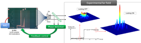 |
| Figure 1: (Left) Schematic of the CBC experiment layout with the PIC. MO: master oscillator; FA: fiber array; MLA: microlens array. (Right) Experimental measurement of the output combined beams in the far field, in closed loop and open-loop configurations. The plot shows the evolution in time of the energy encircled in the main central lobe. |
Abstract:
CEA-Leti and its partners in the European FP7 project PLAT4M today announced they have built three silicon photonics platforms. The four-year project, which launched in 2013, aims at building a European-based supply chain in silicon photonics and speeding industrialization of the technology. PLAT4M, which is funded by a European Commission grant of 10.2 million euros, includes 15 leading European R&D institutes and CMOS companies, key industrial and research organizations in design and packaging, as well as end users in different application fields, to build the complete supply chain.
Leti and Partners in Silicon Photonics Supply-Chain Project Announce Developments on Three Mature Platforms: PLAT4M Project Focused on Speeding Industrialization of the Technology
Grenoble, France | Posted on November 18th, 2015Midway through the project, the consortium has developed advanced technologies and tools by building a coherent design flow, demonstrating manufacturability of elementary devices and process integration, and developing a packaging toolkit. The supply chain is based on technology platforms of Leti, imec and STMicroelectronics, supported by a unified design environment. The high level of maturity of the technology offered by these platforms makes them readily accessible to a broad circle of users in a fabless model.
Imec�s silicon photonics platform, based on 200mm substrates, has matured thanks to the PLAT4M project. The platform is based on SOI substrates with 220nm crystalline silicon on a 2,000nm buried oxide. During this project the existing fabrication processes and integration flow have been fine tuned to have stable and repeatable performance for all photonics building blocks (couplers, waveguides, phase shifters, photodetectors). This feeds the process design kit�s robust performance specifications and guarantees quality and first-time-right designs for the platform�s fabless users for high data-rate telecom and non-telecom applications. PLAT4M partners Thales, Polytec and TNO already are using the technology.
Beyond the 200mm platform, imec has pushed the limits of silicon photonics, exploiting advanced optical lithography with its 193nm immersion lithography scanner. It also has demonstrated very low propagation loss (~0.6dB/cm) for fully etched waveguides with excellent within-wafer linewidth control (standard deviation <3nm for 450nm-wide waveguides) and sub-100nm features. Deep sub-wavelength features can be made in a manufacturable process, avoiding the use of e-beam lithography with this technology.
Using the imec platform, Thales demonstrated a coherent combination of laser beams (CBC). Ultimately, this application aims at producing high-power, high-energy laser sources for sensing, industry or fundamental physics. The CBC rationale is to push the limits of single laser emitters (typically fiber amplifiers) by using a large number of amplifiers and coherently adding the output beams. The coherent addition requires locking the phase of all the amplifying channels. With the number of channels, potentially very large (from tens to thousands), an integrated technology is a major concern in terms of possible industrial products. The first generation CBC demonstrator of PLAT4M, which was packaged by Tyndall UCC, included a one-to-16 channel splitter tree, plus 16 independent thermal phase modulators. The CBC experiment showed the successful coherent addition of 16 laser beams at 1.55�m.
Leti has developed a new photonic platform based on 200mm SOI wafers. This process offers multilevel silicon patterning that allows the design of various passive and active devices (e.g. modulator and photodiode) with thermal tuning capability. Two AlCu levels are available for routing. A process design kit (PDK) is available for circuit design and an MPW service will be proposed in 2016. State-of-the-art performances have been demonstrated: insertion losses are below 2dB/cm for monomode waveguide and below 0.2dB/cm for multimode devices. Germanium photodiode responsivity is > 0.75A/W for a bandwidth >30GHz. Mach-Zehnder modulator VpLp is in the 2V.cm range for 2V operation with an E/O bandwidth > 25GHz. Moreover, Leti and III-V Lab have developed integrated hybrid III-V lasers and electro-absorption modulators (EAM) on silicon using a wafer-bonding technique. The hybrid lasers operate in the single-mode regime and the EAMs exhibit an extinction ratio higher than 20 dB with a drive voltage lower than 2V. Clear eye diagram has been achieved at a bit-rate of 25 Gb/s, confirming strong potential for telecom applications.
During the project, ST developed an additional silicon-photonic platform in 300mm technology to be used as an R&D tool for proof-of-concept purposes. The technology, called DAPHNE (Datacom Advanced PHotonic Nanoscale Environment), is designed for evaluating new devices and subsystems for demonstration. DAPHNE is a flexible platform that perfectly fits R&D needs. While developing it, ST demonstrated wavelength-division-multiplexing solutions using arrayed waveguide gratings, echelle gratings, cascaded Mach-Zehnder interferometers and side-coupled integrated spaced sequence of resonators. Some of the configurations are designed for the 100GBase-LR4 standard, and the experimental characterization results show insertion losses below 0.5dB and channel cross-talks above 25dB for a band flatness of 2nm. Furthermore, proper operation of receiver-and-transmitter blocks to be interfaced to optical devices above them has been demonstrated at 28Gbps, making use of 65nm-node technologies.
The PLAT4M WP2 work has led to a qualitative leap of the design flow for silicon photonics, allowing the photonics community to design more complex and more robust circuits. The electronics OpenAccess standard for data sharing between design-automation tools includes an extension for silicon photonics in a beta phase today. Simulation capabilities were leveraged thanks to an extensive characterization effort from the three partner fabs and thanks to the statistical data gathered for variability prediction. Paris-Sud University has studied theoretically the behavior of different phase shifters and photodetectors for a time-efficient and precise modeling. Mentor Graphics and PhoeniX Software partners have improved phase-aware routing and tool interoperability. Verification and manufacturability have reached industry-requirement standards thanks to the development of new techniques based upon the Mentor Graphics� Calibre� platform that delivers layout-versus-schematic comparison (Calibre nmLVS�), photonic rule checks (PRC) and curvilinear-aware design-rule checks (Calibre nmDRC�). Mask preparation is also improving with better pattern-density control and mask correction.
####
About PLAT4M Consortium Members
Coordinated by Leti, the consortium consists of renowned technology providers, research institutes, end users and SMEs with excellent track records in advanced photonics technologies. At the design and process level, Leti and imec have been the most prominent European players in silicon photonics for a decade. Together with University of Paris-Sud, III-V Lab and TNO, they have demonstrated numerous scientific and technological breakthroughs. For building a complete design flow, Mentor Graphics, PhoeniX BV and Si2 are world leaders in EDA tools and work together to develop a common reference platform.
STMicroelectronics (France and Italy) brings its vast experience in microelectronics, and it has been engaged for the past year in the development of silicon photonics at the industrial level. Tyndall-UCC and Aifotec are renowned experts in the field of optoelectronic packaging and work together on the implementation of packaging technologies developed within PLAT4M in a manufacturing environment.
End-users like Polytec and Thales Research & Technology are driving the demonstrators� development and assessing the use of silicon photonics in their applications fields.
For more information, please click here
Contacts:
Press contact
Agency
+33 6 74 93 23 47
Copyright © PLAT4M Consortium Members
If you have a comment, please Contact us.Issuers of news releases, not 7th Wave, Inc. or Nanotechnology Now, are solely responsible for the accuracy of the content.
Bookmark:


| Related News Press |
News and information
![]() Simulating magnetization in a Heisenberg quantum spin chain April 5th, 2024
Simulating magnetization in a Heisenberg quantum spin chain April 5th, 2024
![]() NRL charters Navy�s quantum inertial navigation path to reduce drift April 5th, 2024
NRL charters Navy�s quantum inertial navigation path to reduce drift April 5th, 2024
![]() Discovery points path to flash-like memory for storing qubits: Rice find could hasten development of nonvolatile quantum memory April 5th, 2024
Discovery points path to flash-like memory for storing qubits: Rice find could hasten development of nonvolatile quantum memory April 5th, 2024
Chip Technology
![]() Discovery points path to flash-like memory for storing qubits: Rice find could hasten development of nonvolatile quantum memory April 5th, 2024
Discovery points path to flash-like memory for storing qubits: Rice find could hasten development of nonvolatile quantum memory April 5th, 2024
![]() Utilizing palladium for addressing contact issues of buried oxide thin film transistors April 5th, 2024
Utilizing palladium for addressing contact issues of buried oxide thin film transistors April 5th, 2024
![]() HKUST researchers develop new integration technique for efficient coupling of III-V and silicon February 16th, 2024
HKUST researchers develop new integration technique for efficient coupling of III-V and silicon February 16th, 2024
Announcements
![]() NRL charters Navy�s quantum inertial navigation path to reduce drift April 5th, 2024
NRL charters Navy�s quantum inertial navigation path to reduce drift April 5th, 2024
![]() Discovery points path to flash-like memory for storing qubits: Rice find could hasten development of nonvolatile quantum memory April 5th, 2024
Discovery points path to flash-like memory for storing qubits: Rice find could hasten development of nonvolatile quantum memory April 5th, 2024
Photonics/Optics/Lasers
![]() With VECSELs towards the quantum internet Fraunhofer: IAF achieves record output power with VECSEL for quantum frequency converters April 5th, 2024
With VECSELs towards the quantum internet Fraunhofer: IAF achieves record output power with VECSEL for quantum frequency converters April 5th, 2024
![]() Nanoscale CL thermometry with lanthanide-doped heavy-metal oxide in TEM March 8th, 2024
Nanoscale CL thermometry with lanthanide-doped heavy-metal oxide in TEM March 8th, 2024
![]() Optically trapped quantum droplets of light can bind together to form macroscopic complexes March 8th, 2024
Optically trapped quantum droplets of light can bind together to form macroscopic complexes March 8th, 2024
![]() HKUST researchers develop new integration technique for efficient coupling of III-V and silicon February 16th, 2024
HKUST researchers develop new integration technique for efficient coupling of III-V and silicon February 16th, 2024
Alliances/Trade associations/Partnerships/Distributorships
![]() Chicago Quantum Exchange welcomes six new partners highlighting quantum technology solutions, from Chicago and beyond September 23rd, 2022
Chicago Quantum Exchange welcomes six new partners highlighting quantum technology solutions, from Chicago and beyond September 23rd, 2022
![]() University of Illinois Chicago joins Brookhaven Lab's Quantum Center June 10th, 2022
University of Illinois Chicago joins Brookhaven Lab's Quantum Center June 10th, 2022
Research partnerships
![]() Discovery points path to flash-like memory for storing qubits: Rice find could hasten development of nonvolatile quantum memory April 5th, 2024
Discovery points path to flash-like memory for storing qubits: Rice find could hasten development of nonvolatile quantum memory April 5th, 2024
![]() Researchers� approach may protect quantum computers from attacks March 8th, 2024
Researchers� approach may protect quantum computers from attacks March 8th, 2024
![]() 'Sudden death' of quantum fluctuations defies current theories of superconductivity: Study challenges the conventional wisdom of superconducting quantum transitions January 12th, 2024
'Sudden death' of quantum fluctuations defies current theories of superconductivity: Study challenges the conventional wisdom of superconducting quantum transitions January 12th, 2024
|
|
||
|
|
||
| The latest news from around the world, FREE | ||
|
|
||
|
|
||
| Premium Products | ||
|
|
||
|
Only the news you want to read!
Learn More |
||
|
|
||
|
Full-service, expert consulting
Learn More |
||
|
|
||