Home > Press > Stanford team combines logic, memory to build a 'high-rise' chip: Today circuit cards are laid out like single-story towns; Futuristic architecture builds layers of logic and memory into skyscraper chips that would be smaller, faster, cheaper -- and taller
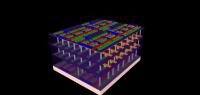 |
| This illustration represents the four-layer prototype high-rise chip built by Stanford engineers. The bottom and top layers are logic transistors. Sandwiched between them are two layers of memory. The vertical tubes are nanoscale electronic "elevators" that connect logic and memory, allowing them to work together to solve problems.
Credit: Max Shulaker, Stanford |
Abstract:
Today circuit cards are like cities in which logic chips compute and memory chips store data. When the computer gets busy, the wires connecting logic and memory get jammed. The Stanford approach would build layers of logic atop layers of memory to create tightly interconnected high-rise chips. Many thousands of nanoscale electronic 'elevators' would move data between the layers faster, using less electricity, than the bottle-neck prone wires connecting single-story logic and memory chips today.
Stanford team combines logic, memory to build a 'high-rise' chip: Today circuit cards are laid out like single-story towns; Futuristic architecture builds layers of logic and memory into skyscraper chips that would be smaller, faster, cheaper -- and taller
Stanford, CA | Posted on December 15th, 2014For decades, the mantra of electronics has been smaller, faster, cheaper.
Today, Stanford engineers add a fourth word - taller.
At a conference in San Francisco, a Stanford team will reveal how to build high-rise chips that could leapfrog the performance of the single-story logic and memory chips on today's circuit cards.
Those circuit cards are like busy cities in which logic chips compute and memory chips store data. But when the computer gets busy, the wires connecting logic and memory can get jammed.
The Stanford approach would end these jams by building layers of logic atop layers of memory to create a tightly interconnected high-rise chip. Many thousands of nanoscale electronic "elevators" would move data between the layers much faster, using less electricity, than the bottle-neck prone wires connecting single-story logic and memory chips today.
The work is led by Subhasish Mitra, a Stanford professor of electrical engineering and computer science, and H.-S. Philip Wong, the Williard R. and Inez Kerr Bell Professor in Stanford's School of Engineering. They describe their new high-rise chip architecture in a paper being presented at the IEEE International Electron Devices Meeting on Dec. 15-17.
The researchers' innovation leverages three breakthroughs.
The first is a new technology for creating transistors, those tiny gates that switch electricity on and off to create digital zeroes and ones. The second is a new type of computer memory that lends itself to multi-story fabrication. The third is a technique to build these new logic and memory technologies into high-rise structures in a radically different way than previous efforts to stack chips.
"This research is at an early stage, but our design and fabrication techniques are scalable," Mitra said. "With further development this architecture could lead to computing performance that is much, much greater than anything available today."
Wong said the prototype chip unveiled at IEDM shows how to put logic and memory together into three-dimensional structures that can be mass-produced.
"Paradigm shift is an overused concept, but here it is appropriate," Wong said. "With this new architecture, electronics manufacturers could put the power of a supercomputer in your hand."
Silicon heat
Engineers have been making silicon chips for decades, but the heat emanating from phones and laptops is evidence of a problem. Even when they are switched off, some electricity leaks out of silicon transistors. Users feel that as heat. But at a system level, the leakage drains batteries and wastes electricity.
Researchers have been trying to solve this major problem by creating carbon nanotubes - or CNT - transistors. They are so slender that nearly 2 billion CNTs could fit within a human hair. CNTs should leak less electricity than silicon because their tiny diameters are easier to pinch shut.
Mitra and Wong are presenting a second paper at the conference showing how their team made some of the highest performance CNT transistors ever built.
They did this by solving a big hurdle: packing enough CNTs into a small enough area to make a useful chip.
Until now the standard process used to grow CNTs did not create a sufficient density of these tubes. The Stanford engineers solved this problem by developing an ingenious technique.
They started by growing CNTs the standard way, on round quartz wafers. Then they added their trick. They created what amounts to a metal film that acts like a tape. Using this adhesive process they lifted an entire crop of CNTs off the quartz growth medium and placed it onto a silicon wafer.
This silicon wafer became the foundation of their high-rise chip.
But first they had to fabricate a CNT layer with sufficient density to make a high performance logic device. So they went though this process 13 times, growing a crop of CNTs on the quartz wafer, and then using their transfer technique to lift and deposit these CNTs onto the silicon wafer.
Using this elegant technological fix, they achieved some of the highest density, highest performance CNTs ever made - especially given that they did this in an academic lab with less sophisticated equipment than a commercial fabrication plant.
Moreover, the Stanford team showed that they could perform this technique on more than one layer of logic as they created their high-rise chip.
What about the memory?
Creating high-performance layers of CNT transistors was only part of their innovation. Just as important was their ability to build a new type of memory directly atop each layer of CNTs.
Wong is a world leader in this new memory technology, which he unveiled at last year's IEDM conference.
Unlike today's memory chips, this new storage technology is not based on silicon.
Instead, the Stanford team fabricated memory using titanium nitride, hafnium oxide and platinum. This formed a metal/oxide/metal sandwich. Applying electricity to this three-metal sandwich one way causes it to resist the flow of electricity. Reversing the electric jolt causes the structure to conduct electricity again.
The change from resistive to conductive states is how this new memory technology creates digital zeroes and ones. The change in conductive states also explains its name: resistive random access memory, or RRAM.
Wong designed RRAM to use less energy than current memory, leading to prolonged battery life in mobile devices.
Inventing this new memory technology was also the key to creating the high-rise chip because RRAM can be made at much lower temperatures than silicon memory.
Interconnected layers
Max Shulaker and Tony Wu, Stanford graduate students in electrical engineering, created the techniques behind the four-story high-rise chip unveiled at the conference.
Everything hinged on the low-heat process for making RRAM and CNTs, which enabled them to fabricate each layer of memory directly atop each layer of CNT logic. While making each memory layer, they were able to drill thousands of interconnections into the logic layer below.
This multiplicity of connections is what enables the high-rise chip to avoid the traffic jams on conventional circuit cards.
There is no way to tightly interconnect layers using today's conventional silicon-based logic and memory. That's because it takes so much heat to build a layer of silicon memory - about 1,000 degrees centigrade - that any attempt to do so would melt the logic below.
Previous efforts to stack silicon chips could save space but not avoid the digital traffic jams. That's because each layer would have to be built separately and connected by wires--which would still be prone to traffic jams, unlike the nanoscale elevators in the Stanford design.
####
For more information, please click here
Contacts:
Tom Abate
650-815-1602
Clifton B. Parker
Stanford News Service:
650-725-0224
Copyright © Stanford University
If you have a comment, please Contact us.Issuers of news releases, not 7th Wave, Inc. or Nanotechnology Now, are solely responsible for the accuracy of the content.
Bookmark:


| Related News Press |
News and information
![]() Simulating magnetization in a Heisenberg quantum spin chain April 5th, 2024
Simulating magnetization in a Heisenberg quantum spin chain April 5th, 2024
![]() NRL charters Navy�s quantum inertial navigation path to reduce drift April 5th, 2024
NRL charters Navy�s quantum inertial navigation path to reduce drift April 5th, 2024
![]() Discovery points path to flash-like memory for storing qubits: Rice find could hasten development of nonvolatile quantum memory April 5th, 2024
Discovery points path to flash-like memory for storing qubits: Rice find could hasten development of nonvolatile quantum memory April 5th, 2024
Chip Technology
![]() Discovery points path to flash-like memory for storing qubits: Rice find could hasten development of nonvolatile quantum memory April 5th, 2024
Discovery points path to flash-like memory for storing qubits: Rice find could hasten development of nonvolatile quantum memory April 5th, 2024
![]() Utilizing palladium for addressing contact issues of buried oxide thin film transistors April 5th, 2024
Utilizing palladium for addressing contact issues of buried oxide thin film transistors April 5th, 2024
![]() HKUST researchers develop new integration technique for efficient coupling of III-V and silicon February 16th, 2024
HKUST researchers develop new integration technique for efficient coupling of III-V and silicon February 16th, 2024
Memory Technology
![]() Utilizing palladium for addressing contact issues of buried oxide thin film transistors April 5th, 2024
Utilizing palladium for addressing contact issues of buried oxide thin film transistors April 5th, 2024
![]() Interdisciplinary: Rice team tackles the future of semiconductors Multiferroics could be the key to ultralow-energy computing October 6th, 2023
Interdisciplinary: Rice team tackles the future of semiconductors Multiferroics could be the key to ultralow-energy computing October 6th, 2023
![]() Researchers discover materials exhibiting huge magnetoresistance June 9th, 2023
Researchers discover materials exhibiting huge magnetoresistance June 9th, 2023
Discoveries
![]() Chemical reactions can scramble quantum information as well as black holes April 5th, 2024
Chemical reactions can scramble quantum information as well as black holes April 5th, 2024
![]() New micromaterial releases nanoparticles that selectively destroy cancer cells April 5th, 2024
New micromaterial releases nanoparticles that selectively destroy cancer cells April 5th, 2024
![]() Utilizing palladium for addressing contact issues of buried oxide thin film transistors April 5th, 2024
Utilizing palladium for addressing contact issues of buried oxide thin film transistors April 5th, 2024
Announcements
![]() NRL charters Navy�s quantum inertial navigation path to reduce drift April 5th, 2024
NRL charters Navy�s quantum inertial navigation path to reduce drift April 5th, 2024
![]() Discovery points path to flash-like memory for storing qubits: Rice find could hasten development of nonvolatile quantum memory April 5th, 2024
Discovery points path to flash-like memory for storing qubits: Rice find could hasten development of nonvolatile quantum memory April 5th, 2024
Interviews/Book Reviews/Essays/Reports/Podcasts/Journals/White papers/Posters
![]() Simulating magnetization in a Heisenberg quantum spin chain April 5th, 2024
Simulating magnetization in a Heisenberg quantum spin chain April 5th, 2024
![]() Discovery points path to flash-like memory for storing qubits: Rice find could hasten development of nonvolatile quantum memory April 5th, 2024
Discovery points path to flash-like memory for storing qubits: Rice find could hasten development of nonvolatile quantum memory April 5th, 2024
Events/Classes
![]() Researchers demonstrate co-propagation of quantum and classical signals: Study shows that quantum encryption can be implemented in existing fiber networks January 20th, 2023
Researchers demonstrate co-propagation of quantum and classical signals: Study shows that quantum encryption can be implemented in existing fiber networks January 20th, 2023
|
|
||
|
|
||
| The latest news from around the world, FREE | ||
|
|
||
|
|
||
| Premium Products | ||
|
|
||
|
Only the news you want to read!
Learn More |
||
|
|
||
|
Full-service, expert consulting
Learn More |
||
|
|
||