Home > Press > High photosensitivity 2D-few-layered molybdenum diselenide phototransistors
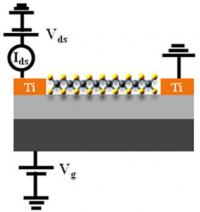 |
| This is the schematic structure of the few-layered MoSe2 FETs.
Credit: copyright (c) 2014 Toyohashi University of Technology. All rights reserved. |
Abstract:
Two-dimensional (2D) layered materials are now attracting a lot of interest due to their unique optoelectronic properties at atomic thicknesses. Among them, graphene has been mostly investigated, but the zero-gap nature of graphene limits its practical applications. Therefore, 2D layered materials with intrinsic band gaps such as MoS2, MoSe2, and MoTe2 are of interest as promising candidates for ultrathin and high-performance optoelectronic devices
High photosensitivity 2D-few-layered molybdenum diselenide phototransistors
Toyohashi, Japan | Posted on December 8th, 2014Here, Pil Ju Ko and colleagues at Toyohashi University of Technology, Japan have fabricated back-gated field-effect phototransistors made of MoSe2 crystals having a thickness of only twenty nanometers. The devices were fabricated by mechanical cleavage of MoSe2 crystals into few-layered flakes, followed by transfer onto a silicon wafer with pre-deposited titanium electrodes.
Despite their ultra-thin physical size, the devices showed excellent field-effect phototransistor characteristics. The measured photoresponsivity of 97.1 AW-1 at zero back gate voltage was higher than previous reports of photodetectors fabricated using GaS, GaSe, MoS2, and InSe. The photoresponse of the MoSe2 was much faster (less than 15 msec) than ultrasensitive photodetectors based on monolayer MoS2. Furthermore, the theoretical external quantum efficiency was 280-fold higher than of commercial Si and InGaAs photodiodes.
The research shows that MoSe2 is a promising material for photodetector applications. The group is optimization the device performance by studying thickness-dependent of the photosensitivity.
Reference:
Authors: Abdelkader Abderrahmane, Pil Ju Ko, Tran Viet Thu, Shunji Ishizawa, Tsukasa Takamura and Adarsh Sandhu.
Title of original paper: High photosensitivity few-layered MoSe2 back-gated field-effect phototransistors.
Journal, volume, pages and year: Nanotechnology 25 365202 (1-5) (2014).
Digital Object Identifier (DOI): 10.1088/0957-4484/25/36/365202.
Affiliations: Electronics-Inspired Interdisciplinary Research Institute (EIIRIS) and Department of Electrical and Electronic Information Engineering, Toyohashi University of Technology, 1-1 Hibarigaoka, Tempaku, Toyohashi, Aichi 441-8580, Japan
####
About Toyohashi University of Technology
Founded in 1976 as a National University of Japan, Toyohashi University of Technology is a vibrant modern institute with research activities reflecting the modern era of advanced electronics, engineering, and life sciences.
For more information, please click here
Contacts:
Toyohashi University of Technology
1-1 Hibarigaoka, Tempaku
Toyohashi, Aichi Prefecture, 441-8580, JAPAN
Inquiries: Committee for Public Relations
Michiteru Kitazaki
Copyright © Toyohashi University of Technology
If you have a comment, please Contact us.Issuers of news releases, not 7th Wave, Inc. or Nanotechnology Now, are solely responsible for the accuracy of the content.
Bookmark:


| Related Links |
| Related News Press |
News and information
![]() Simulating magnetization in a Heisenberg quantum spin chain April 5th, 2024
Simulating magnetization in a Heisenberg quantum spin chain April 5th, 2024
![]() NRL charters Navy�s quantum inertial navigation path to reduce drift April 5th, 2024
NRL charters Navy�s quantum inertial navigation path to reduce drift April 5th, 2024
![]() Discovery points path to flash-like memory for storing qubits: Rice find could hasten development of nonvolatile quantum memory April 5th, 2024
Discovery points path to flash-like memory for storing qubits: Rice find could hasten development of nonvolatile quantum memory April 5th, 2024
![]() Good as gold - improving infectious disease testing with gold nanoparticles April 5th, 2024
Good as gold - improving infectious disease testing with gold nanoparticles April 5th, 2024
Display technology/LEDs/SS Lighting/OLEDs
![]() Utilizing palladium for addressing contact issues of buried oxide thin film transistors April 5th, 2024
Utilizing palladium for addressing contact issues of buried oxide thin film transistors April 5th, 2024
Graphene/ Graphite
![]() NRL discovers two-dimensional waveguides February 16th, 2024
NRL discovers two-dimensional waveguides February 16th, 2024
Flexible Electronics
Chip Technology
![]() Discovery points path to flash-like memory for storing qubits: Rice find could hasten development of nonvolatile quantum memory April 5th, 2024
Discovery points path to flash-like memory for storing qubits: Rice find could hasten development of nonvolatile quantum memory April 5th, 2024
![]() Utilizing palladium for addressing contact issues of buried oxide thin film transistors April 5th, 2024
Utilizing palladium for addressing contact issues of buried oxide thin film transistors April 5th, 2024
![]() HKUST researchers develop new integration technique for efficient coupling of III-V and silicon February 16th, 2024
HKUST researchers develop new integration technique for efficient coupling of III-V and silicon February 16th, 2024
Optical computing/Photonic computing
![]() With VECSELs towards the quantum internet Fraunhofer: IAF achieves record output power with VECSEL for quantum frequency converters April 5th, 2024
With VECSELs towards the quantum internet Fraunhofer: IAF achieves record output power with VECSEL for quantum frequency converters April 5th, 2024
![]() Chemical reactions can scramble quantum information as well as black holes April 5th, 2024
Chemical reactions can scramble quantum information as well as black holes April 5th, 2024
![]() Optically trapped quantum droplets of light can bind together to form macroscopic complexes March 8th, 2024
Optically trapped quantum droplets of light can bind together to form macroscopic complexes March 8th, 2024
![]() HKUST researchers develop new integration technique for efficient coupling of III-V and silicon February 16th, 2024
HKUST researchers develop new integration technique for efficient coupling of III-V and silicon February 16th, 2024
Discoveries
![]() Chemical reactions can scramble quantum information as well as black holes April 5th, 2024
Chemical reactions can scramble quantum information as well as black holes April 5th, 2024
![]() New micromaterial releases nanoparticles that selectively destroy cancer cells April 5th, 2024
New micromaterial releases nanoparticles that selectively destroy cancer cells April 5th, 2024
![]() Utilizing palladium for addressing contact issues of buried oxide thin film transistors April 5th, 2024
Utilizing palladium for addressing contact issues of buried oxide thin film transistors April 5th, 2024
Announcements
![]() NRL charters Navy�s quantum inertial navigation path to reduce drift April 5th, 2024
NRL charters Navy�s quantum inertial navigation path to reduce drift April 5th, 2024
![]() Discovery points path to flash-like memory for storing qubits: Rice find could hasten development of nonvolatile quantum memory April 5th, 2024
Discovery points path to flash-like memory for storing qubits: Rice find could hasten development of nonvolatile quantum memory April 5th, 2024
Interviews/Book Reviews/Essays/Reports/Podcasts/Journals/White papers/Posters
![]() Simulating magnetization in a Heisenberg quantum spin chain April 5th, 2024
Simulating magnetization in a Heisenberg quantum spin chain April 5th, 2024
![]() Discovery points path to flash-like memory for storing qubits: Rice find could hasten development of nonvolatile quantum memory April 5th, 2024
Discovery points path to flash-like memory for storing qubits: Rice find could hasten development of nonvolatile quantum memory April 5th, 2024
Quantum nanoscience
![]() Simulating magnetization in a Heisenberg quantum spin chain April 5th, 2024
Simulating magnetization in a Heisenberg quantum spin chain April 5th, 2024
![]() Optically trapped quantum droplets of light can bind together to form macroscopic complexes March 8th, 2024
Optically trapped quantum droplets of light can bind together to form macroscopic complexes March 8th, 2024
![]() Bridging light and electrons January 12th, 2024
Bridging light and electrons January 12th, 2024
![]() 'Sudden death' of quantum fluctuations defies current theories of superconductivity: Study challenges the conventional wisdom of superconducting quantum transitions January 12th, 2024
'Sudden death' of quantum fluctuations defies current theories of superconductivity: Study challenges the conventional wisdom of superconducting quantum transitions January 12th, 2024
|
|
||
|
|
||
| The latest news from around the world, FREE | ||
|
|
||
|
|
||
| Premium Products | ||
|
|
||
|
Only the news you want to read!
Learn More |
||
|
|
||
|
Full-service, expert consulting
Learn More |
||
|
|
||