Home > Press > New Material Allows for Ultra-Thin Solar Cells
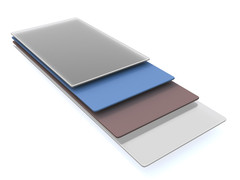 |
| The solar cell's layer system: two semiconductor layers in the middle, connected to electrodes on either side. |
Abstract:
Scientists at the Vienna University of Technology have managed to combine two semiconductor materials, consisting of only three atomic layers each. This new structure holds great promise for a new kinds of solar cell.
New Material Allows for Ultra-Thin Solar Cells
Vienna, Austria | Posted on August 4th, 2014Extremely thin, semi-transparent, flexible solar cells could soon become reality. At the Vienna University of Technology, Thomas Mueller, Marco Furchi and Andreas Pospischil have managed to create a semiconductor structure consisting of two ultra-thin layers, which appears to be excellently suited for photovoltaic energy conversion
Several months ago, the team had already produced an ultra-thin layer of the photoactive crystal tungsten diselenide. Now, this semiconductor has successfully been combined with another layer made of molybdenum disulphide, creating a designer-material that may be used in future low-cost solar cells. With this advance, the researchers hope to establish a new kind of solar cell technology.
Two-Dimensional Structures
Ultra-thin materials, which consist only of one or a few atomic layers are currently a hot topic in materials science today. Research on two-dimensional materials started with graphene, a material made of a single layer of carbon atoms. Like other research groups all over the world, Thomas Mueller and his team acquired the necessary know-how to handle, analyse and improve ultra-thin layers by working with graphene. This know-how has now been applied to other ultra-thin materials.
"Quite often, two-dimensional crystals have electronic properties that are completely different from those of thicker layers of the same material", says Thomas Mueller. His team was the first to combine two different ultra-thin semiconductor layers and study their optoelectronic properties.
Two Layers with Different Functions
Tungsten diselenide is a semiconductor which consists of three atomic layers. One layer of tungsten is sandwiched between two layers of selenium atoms. "We had already been able to show that tungsten diselenide can be used to turn light into electric energy and vice versa", says Thomas Mueller. But a solar cell made only of tungsten diselenide would require countless tiny metal electrodes tightly spaced only a few micrometers apart. If the material is combined with molybdenium disulphide, which also consists of three atomic layers, this problem is elegantly circumvented. The heterostructure can now be used to build large-area solar cells.
When light shines on a photoactive material single electrons are removed from their original position. A positively charged hole remains, where the electron used to be. Both the electron and the hole can move freely in the material, but they only contribute to the electrical current when they are kept apart so that they cannot recombine.
To prevent recombination of electrons and holes, metallic electrodes can be used, through which the charge is sucked away - or a second material is added. "The holes move inside the tungsten diselenide layer, the electrons, on the other hand, migrate into the molybednium disulphide", says Thomas Mueller. Thus, recombination is suppressed.
This is only possible if the energies of the electrons in both layers are tuned exactly the right way. In the experiment, this can be done using electrostatic fields. Florian Libisch and Professor Joachim Burgd�rfer (TU Vienna) provided computer simulations to calculate how the energy of the electrons changes in both materials and which voltage leads to an optimum yield of electrical power.
Tightly Packed Layers
"One of the greatest challenges was to stack the two materials, creating an atomically flat structure", says Thomas Mueller. "If there are any molecules between the two layers, so that there is no direct contact, the solar cell will not work." Eventually, this feat was accomplished by heating both layers in vacuum and stacking it in ambient atmosphere. Water between the two layers was removed by heating the layer structure once again.
Part of the incoming light passes right through the material. The rest is absorbed and converted into electric energy. The material could be used for glass fronts, letting most of the light in, but still creating electricity. As it only consists of a few atomic layers, it is extremely light weight (300 square meters weigh only one gram), and very flexible. Now the team is working on stacking more than two layers - this will reduce transparency, but increase the electrical power.
####
For more information, please click here
Contacts:
Florian Aigner
43-158-801-41027
Copyright © Vienna University of Technology
If you have a comment, please Contact us.Issuers of news releases, not 7th Wave, Inc. or Nanotechnology Now, are solely responsible for the accuracy of the content.
Bookmark:


| Related Links |
![]() Original publication in �Nano Letters�:
Original publication in �Nano Letters�:
| Related News Press |
News and information
![]() Simulating magnetization in a Heisenberg quantum spin chain April 5th, 2024
Simulating magnetization in a Heisenberg quantum spin chain April 5th, 2024
![]() NRL charters Navy�s quantum inertial navigation path to reduce drift April 5th, 2024
NRL charters Navy�s quantum inertial navigation path to reduce drift April 5th, 2024
![]() Discovery points path to flash-like memory for storing qubits: Rice find could hasten development of nonvolatile quantum memory April 5th, 2024
Discovery points path to flash-like memory for storing qubits: Rice find could hasten development of nonvolatile quantum memory April 5th, 2024
![]() Good as gold - improving infectious disease testing with gold nanoparticles April 5th, 2024
Good as gold - improving infectious disease testing with gold nanoparticles April 5th, 2024
Thin films
![]() Utilizing palladium for addressing contact issues of buried oxide thin film transistors April 5th, 2024
Utilizing palladium for addressing contact issues of buried oxide thin film transistors April 5th, 2024
![]() Understanding the mechanism of non-uniform formation of diamond film on tools: Paving the way to a dry process with less environmental impact March 24th, 2023
Understanding the mechanism of non-uniform formation of diamond film on tools: Paving the way to a dry process with less environmental impact March 24th, 2023
![]() New study introduces the best graphite films: The work by Distinguished Professor Feng Ding at UNIST has been published in the October 2022 issue of Nature Nanotechnology November 4th, 2022
New study introduces the best graphite films: The work by Distinguished Professor Feng Ding at UNIST has been published in the October 2022 issue of Nature Nanotechnology November 4th, 2022
Discoveries
![]() Chemical reactions can scramble quantum information as well as black holes April 5th, 2024
Chemical reactions can scramble quantum information as well as black holes April 5th, 2024
![]() New micromaterial releases nanoparticles that selectively destroy cancer cells April 5th, 2024
New micromaterial releases nanoparticles that selectively destroy cancer cells April 5th, 2024
![]() Utilizing palladium for addressing contact issues of buried oxide thin film transistors April 5th, 2024
Utilizing palladium for addressing contact issues of buried oxide thin film transistors April 5th, 2024
Announcements
![]() NRL charters Navy�s quantum inertial navigation path to reduce drift April 5th, 2024
NRL charters Navy�s quantum inertial navigation path to reduce drift April 5th, 2024
![]() Discovery points path to flash-like memory for storing qubits: Rice find could hasten development of nonvolatile quantum memory April 5th, 2024
Discovery points path to flash-like memory for storing qubits: Rice find could hasten development of nonvolatile quantum memory April 5th, 2024
Interviews/Book Reviews/Essays/Reports/Podcasts/Journals/White papers/Posters
![]() Simulating magnetization in a Heisenberg quantum spin chain April 5th, 2024
Simulating magnetization in a Heisenberg quantum spin chain April 5th, 2024
![]() Discovery points path to flash-like memory for storing qubits: Rice find could hasten development of nonvolatile quantum memory April 5th, 2024
Discovery points path to flash-like memory for storing qubits: Rice find could hasten development of nonvolatile quantum memory April 5th, 2024
Energy
![]() Development of zinc oxide nanopagoda array photoelectrode: photoelectrochemical water-splitting hydrogen production January 12th, 2024
Development of zinc oxide nanopagoda array photoelectrode: photoelectrochemical water-splitting hydrogen production January 12th, 2024
![]() Shedding light on unique conduction mechanisms in a new type of perovskite oxide November 17th, 2023
Shedding light on unique conduction mechanisms in a new type of perovskite oxide November 17th, 2023
![]() Inverted perovskite solar cell breaks 25% efficiency record: Researchers improve cell efficiency using a combination of molecules to address different November 17th, 2023
Inverted perovskite solar cell breaks 25% efficiency record: Researchers improve cell efficiency using a combination of molecules to address different November 17th, 2023
![]() The efficient perovskite cells with a structured anti-reflective layer � another step towards commercialization on a wider scale October 6th, 2023
The efficient perovskite cells with a structured anti-reflective layer � another step towards commercialization on a wider scale October 6th, 2023
Solar/Photovoltaic
![]() Development of zinc oxide nanopagoda array photoelectrode: photoelectrochemical water-splitting hydrogen production January 12th, 2024
Development of zinc oxide nanopagoda array photoelectrode: photoelectrochemical water-splitting hydrogen production January 12th, 2024
![]() Shedding light on unique conduction mechanisms in a new type of perovskite oxide November 17th, 2023
Shedding light on unique conduction mechanisms in a new type of perovskite oxide November 17th, 2023
![]() Inverted perovskite solar cell breaks 25% efficiency record: Researchers improve cell efficiency using a combination of molecules to address different November 17th, 2023
Inverted perovskite solar cell breaks 25% efficiency record: Researchers improve cell efficiency using a combination of molecules to address different November 17th, 2023
![]() Charged �molecular beasts� the basis for new compounds: Researchers at Leipzig University use �aggressive� fragments of molecular ions for chemical synthesis November 3rd, 2023
Charged �molecular beasts� the basis for new compounds: Researchers at Leipzig University use �aggressive� fragments of molecular ions for chemical synthesis November 3rd, 2023
|
|
||
|
|
||
| The latest news from around the world, FREE | ||
|
|
||
|
|
||
| Premium Products | ||
|
|
||
|
Only the news you want to read!
Learn More |
||
|
|
||
|
Full-service, expert consulting
Learn More |
||
|
|
||