Home > Press > High Quality Three-Dimensional Nanoporous Graphene
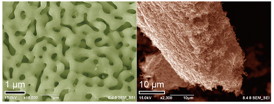 |
| Nanoporous graphene on nanoporous Ni (left) and Nanoporous graphene after dissolving the nanoporous Ni substrate. |
Abstract:
Three-dimentional (3D) nanoporous graphene with preserved 2D Dirac electronic characters was successfully synthesized by Dr. Yoshikazu Ito and Prof. Mingwei CHEN at Advanced Institute for Materials Research, Tohoku University. The nanoporous graphene is constructed by a single layer graphene sheet that is continuously inter-connected to form a complex 3D network structure. This free-standing nanoporous graphene with an excellent crystallinity possesses high mobility, holding great promise for the applications in electronic devices.
High Quality Three-Dimensional Nanoporous Graphene
Katahira, Japan | Posted on May 2nd, 2014The nanoporous graphene were grown by a nanoporous metal based chemical vapor deposition (CVD) method as shown in Figure 1(a). The overall morphology of the nanoporous graphene in Figure 1(b) shows a ~20 �m thick free-standing bulk sheet. Although the 3D nanoporous graphene has a complex structure, it is demonstrated to be 500 cm2/Vs in electron mobility and a mass-less Dirac cone system. As the conventional transistor requires electron mobility of 200 cm2/Vs, it is greatly expected that this nanoporous graphene will bring a new device which can be replaced with Si devices.
This work is collaborated with the research teams of Prof. Katsumi Tanigaki and Prof. Takashi Takahashi at AIMR, Tohoku University. This research results will be published in issue 19 of 'Angewandte Chemie International Edition' as a Hot Paper on 2 May.
Introduction
Graphene is a mono-layer carbon material with low cost, high chemical/thermal stability, and ultrahigh strength and is expected to be a replacement of silicon and noble metals for electron devices, battery materials, photo-/ion detectors and catalysts. Although some of graphene products such as display and electrodes are commercially available, the applications are limited due to the 2D sheet structure. In other words, the performance per gram is excellent but the performance per volume cannot be achieved easily. Therefore, many efforts have been made to construct the 2D material as a 3D structure with retained physical/chemical properties and high volumetric performance. However, the reported 3D nanoporous carbon materials suffer from poor mobility because of the lower crystallinity, which cannot be used for the electron devices. To achieve semiconductor-grade 3D carbon materials, the monolayer graphene sheet with a high crystalline structure is required in a 3D structure. Thus, we have developed a 3D nanoporous graphene with preserved high mobility and unique 2D electronic properties of graphene.
Research content
The nanoporous graphene in Figure 1 were synthesized by the nanoporous metal based CVD method. The nanoporous graphene fully inherits the geometric structure of the nanoporous nickel substrate after dissolving nickel. The atomic structure of the nanoporous graphene was observed by TEM as shown in Figure 2. The ligament in Figure 2(a) were constructed by flat surface parts (Figure 2(b)) and curvature parts (Figure 2(c)) of the graphene sheet. It is obvious that the six-membered rings were observed in the flat part while the five- and seven-membered rings were observed in the curved parts due to the geometrical requirement to create the curvature structures.
The physical properties of the nanoporous graphene were investigated. As the 2D graphene is a Dirac cone system (Figure 3(a)) and shows a linear dispersion electronic density of state (Figure 3(b)). The 3D nanoporous graphene in Figure 2 also demonstrates a linear relationship near the Fermi level, which is similar with the 2D graphene. The electron mobility of the nanoporous graphene with different pore sizes was measured. As the temperature increase, the electron mobility slightly decreases to 200-400 cm2/Vs. As compared with 2D CVD graphene, the electron mobility is still high enough for device applications.
In conclusion, the nanoporous graphene preserves 2D graphene futures. These findings are firstly reported for revealing the physical properties of 3D nanoporous graphene.
Future visions
The 3D nanoporous graphene is expected to bring breakthrough of solving a problem of volumetric performance of 2D graphene by providing abundant porous structures for an easy mass transport and large effective surface area. Moreover, the nanoporous graphene preserves 2D graphene electronic characters and expected to be employed for applications in electronic devices such as a transistors and condensers.
Acknowledgement
We appreciate the supports from JST-CREST "Phase Interface Science for Highly Efficient Energy Utilization"; the fusion research funds of "World Premier International (WPI) Research Center Initiative for Atoms, Molecules and Materials", MEXT (Japan).
####
For more information, please click here
Contacts:
Yasufumi Nakamichi
81-222-176-146
About research (experiment and theory)
Mingwei Chen (PI, Professor)
Advanced Institute for Materials Research (AIMR), Tohoku University, Chen group
About Media Relations
Yasufumi Nakamichi (Manager, Assistant Professor)
Advanced Institute for Materials Research (AIMR), Tohoku University, PR & Outreach office
Copyright © Advanced Institute for Materials Research (AIMR), Tohoku Uni
If you have a comment, please Contact us.Issuers of news releases, not 7th Wave, Inc. or Nanotechnology Now, are solely responsible for the accuracy of the content.
Bookmark:


| Related Links |
| Related News Press |
News and information
![]() Researchers develop molecular qubits that communicate at telecom frequencies October 3rd, 2025
Researchers develop molecular qubits that communicate at telecom frequencies October 3rd, 2025
![]() Next-generation quantum communication October 3rd, 2025
Next-generation quantum communication October 3rd, 2025
![]() "Nanoreactor" cage uses visible light for catalytic and ultra-selective cross-cycloadditions October 3rd, 2025
"Nanoreactor" cage uses visible light for catalytic and ultra-selective cross-cycloadditions October 3rd, 2025
Graphene/ Graphite
![]() Electrifying results shed light on graphene foam as a potential material for lab grown cartilage June 6th, 2025
Electrifying results shed light on graphene foam as a potential material for lab grown cartilage June 6th, 2025
![]() Breakthrough in proton barrier films using pore-free graphene oxide: Kumamoto University researchers achieve new milestone in advanced coating technologies September 13th, 2024
Breakthrough in proton barrier films using pore-free graphene oxide: Kumamoto University researchers achieve new milestone in advanced coating technologies September 13th, 2024
Chip Technology
![]() Lab to industry: InSe wafer-scale breakthrough for future electronics August 8th, 2025
Lab to industry: InSe wafer-scale breakthrough for future electronics August 8th, 2025
![]() A 1960s idea inspires NBI researchers to study hitherto inaccessible quantum states June 6th, 2025
A 1960s idea inspires NBI researchers to study hitherto inaccessible quantum states June 6th, 2025
![]() Programmable electron-induced color router array May 14th, 2025
Programmable electron-induced color router array May 14th, 2025
Discoveries
![]() Researchers develop molecular qubits that communicate at telecom frequencies October 3rd, 2025
Researchers develop molecular qubits that communicate at telecom frequencies October 3rd, 2025
![]() Next-generation quantum communication October 3rd, 2025
Next-generation quantum communication October 3rd, 2025
![]() "Nanoreactor" cage uses visible light for catalytic and ultra-selective cross-cycloadditions October 3rd, 2025
"Nanoreactor" cage uses visible light for catalytic and ultra-selective cross-cycloadditions October 3rd, 2025
Materials/Metamaterials/Magnetoresistance
![]() First real-time observation of two-dimensional melting process: Researchers at Mainz University unveil new insights into magnetic vortex structures August 8th, 2025
First real-time observation of two-dimensional melting process: Researchers at Mainz University unveil new insights into magnetic vortex structures August 8th, 2025
![]() Researchers unveil a groundbreaking clay-based solution to capture carbon dioxide and combat climate change June 6th, 2025
Researchers unveil a groundbreaking clay-based solution to capture carbon dioxide and combat climate change June 6th, 2025
![]() A 1960s idea inspires NBI researchers to study hitherto inaccessible quantum states June 6th, 2025
A 1960s idea inspires NBI researchers to study hitherto inaccessible quantum states June 6th, 2025
![]() Institute for Nanoscience hosts annual proposal planning meeting May 16th, 2025
Institute for Nanoscience hosts annual proposal planning meeting May 16th, 2025
Announcements
![]() Rice membrane extracts lithium from brines with greater speed, less waste October 3rd, 2025
Rice membrane extracts lithium from brines with greater speed, less waste October 3rd, 2025
![]() Researchers develop molecular qubits that communicate at telecom frequencies October 3rd, 2025
Researchers develop molecular qubits that communicate at telecom frequencies October 3rd, 2025
![]() Next-generation quantum communication October 3rd, 2025
Next-generation quantum communication October 3rd, 2025
![]() "Nanoreactor" cage uses visible light for catalytic and ultra-selective cross-cycloadditions October 3rd, 2025
"Nanoreactor" cage uses visible light for catalytic and ultra-selective cross-cycloadditions October 3rd, 2025
Interviews/Book Reviews/Essays/Reports/Podcasts/Journals/White papers/Posters
![]() Spinel-type sulfide semiconductors to operate the next-generation LEDs and solar cells For solar-cell absorbers and green-LED source October 3rd, 2025
Spinel-type sulfide semiconductors to operate the next-generation LEDs and solar cells For solar-cell absorbers and green-LED source October 3rd, 2025
![]() Rice membrane extracts lithium from brines with greater speed, less waste October 3rd, 2025
Rice membrane extracts lithium from brines with greater speed, less waste October 3rd, 2025
|
|
||
|
|
||
| The latest news from around the world, FREE | ||
|
|
||
|
|
||
| Premium Products | ||
|
|
||
|
Only the news you want to read!
Learn More |
||
|
|
||
|
Full-service, expert consulting
Learn More |
||
|
|
||