Home > Press > Obducat has launched a new generation of SINDRE® Nano Imprint production system
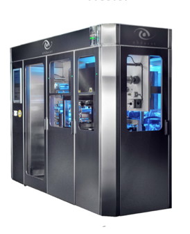 |
| SINDRE 400 G2 |
Abstract:
OBDUCAT, leading manufacturer of lithography solutions based on nanoimprint lithography (NIL), launches 2nd generation SINDRE® with industry-leading productivity. With the improved performance it will represent the most cost effective NIL production solution on the market. The system is based on Obducat's patented SoftPress®, IPS® - and STU® technologies.
Obducat has launched a new generation of SINDRE® Nano Imprint production system
Lund, Sweden | Posted on April 11th, 2014The fully automated SINDRE system, which enables throughputs of up to 60 wafers per hour, provides state-of-the-art performance combined with industry-leading Cost of Ownership (CoO). The new SINDRE integrates the latest advances in manufacturing technology which enables high throughput, high repeatability at a defectivity level which surpass industry requirements. The first system has already been delivered and passed customer final approval in January this year and the next system will be delivered in third quarter this year.
The new SINDRE platform is a fully integrated NIL system which includes integrated fabrication of the Intermediate Polymer Stamp (IPS). This is a proven and reliable process which was also integrated in previous generation of SINDRE systems delivered by Obducat during the last five years. Obducat's patented IPS technology covers the use of a transparent flexible stamp in any kind of imprint process. The use of the IPS technology ensures a long life time of the stampers which minimize the stamp related costs per imprint. The unique and patented SoftPress technology, applied in the system, ensures the necessary level of conformity between the stamp and substrate vital for establishing high imprint uniformity. This enables a large process window for downstream processes leading to a high yield and low CoO. All this has been integrated into a very compact system having a small footprint.
The new SINDRE system also offers a wide flexibility which includes the possibility to use different resists and IPS materials to support customization of the imprint process. Additionally the system can run both UV- as well as thermal based NIL processes, giving the capability to imprint structure sizes ranging from 20nm and upwards, on substrate sizes up to 200 mm in diameter.
"The versatility and superior performance of our patented key technologies has been extended further to safeguard Obducat's continued technological leadership in the NIL industry" says Babak Heidari, CTO of Obducat.
Example of components which are ideally produced with this system are optical, photonic, LEDs, fluidic and other biomedical components.
"Obducat again confirms its leading position with this launch. With more than 130 NIL systems delivered during the last decade and several of these being used for manufacturing purposes in LEDs, photonics and biomedical applications, we are breaking new barriers in terms of performance and cost efficiency" says Patrik Lundström, CEO of Obducat.
####
About Obducat
Obducat AB is an innovative developer and supplier of technologies, products and processes, based on Obducat’s proprietary nanoimprint technology, used for the production and replication of advanced micro and nano structures. Obducat’s products and services are intended to serve the demands of companies within the information storage, semiconductor, printed circuit board, and sensor industries. Obducat has offices in Sweden and China, with the headquarter located in Lund, Sweden. The Obducat shares are publicly traded on the Swedish NGM stock exchange
For more information, please click here
Contacts:
SCHEELEVÄGEN 2
223 81 LUND SWEDEN
TEL +46 46 10 16 00
FAX +46 46 10 16 60
Copyright © Obducat
If you have a comment, please Contact us.Issuers of news releases, not 7th Wave, Inc. or Nanotechnology Now, are solely responsible for the accuracy of the content.
Bookmark:


| Related News Press |
News and information
![]() Decoding hydrogen‑bond network of electrolyte for cryogenic durable aqueous zinc‑ion batteries January 30th, 2026
Decoding hydrogen‑bond network of electrolyte for cryogenic durable aqueous zinc‑ion batteries January 30th, 2026
![]() COF scaffold membrane with gate‑lane nanostructure for efficient Li+/Mg2+ separation January 30th, 2026
COF scaffold membrane with gate‑lane nanostructure for efficient Li+/Mg2+ separation January 30th, 2026
Chip Technology
![]() Metasurfaces smooth light to boost magnetic sensing precision January 30th, 2026
Metasurfaces smooth light to boost magnetic sensing precision January 30th, 2026
![]() Beyond silicon: Electronics at the scale of a single molecule January 30th, 2026
Beyond silicon: Electronics at the scale of a single molecule January 30th, 2026
![]() Lab to industry: InSe wafer-scale breakthrough for future electronics August 8th, 2025
Lab to industry: InSe wafer-scale breakthrough for future electronics August 8th, 2025
Announcements
![]() Decoding hydrogen‑bond network of electrolyte for cryogenic durable aqueous zinc‑ion batteries January 30th, 2026
Decoding hydrogen‑bond network of electrolyte for cryogenic durable aqueous zinc‑ion batteries January 30th, 2026
![]() COF scaffold membrane with gate‑lane nanostructure for efficient Li+/Mg2+ separation January 30th, 2026
COF scaffold membrane with gate‑lane nanostructure for efficient Li+/Mg2+ separation January 30th, 2026
Tools
![]() Metasurfaces smooth light to boost magnetic sensing precision January 30th, 2026
Metasurfaces smooth light to boost magnetic sensing precision January 30th, 2026
![]() From sensors to smart systems: the rise of AI-driven photonic noses January 30th, 2026
From sensors to smart systems: the rise of AI-driven photonic noses January 30th, 2026
![]() Japan launches fully domestically produced quantum computer: Expo visitors to experience quantum computing firsthand August 8th, 2025
Japan launches fully domestically produced quantum computer: Expo visitors to experience quantum computing firsthand August 8th, 2025
Printing/Lithography/Inkjet/Inks/Bio-printing/Dyes
![]() Presenting: Ultrasound-based printing of 3D materials—potentially inside the body December 8th, 2023
Presenting: Ultrasound-based printing of 3D materials—potentially inside the body December 8th, 2023
![]() Simple ballpoint pen can write custom LEDs August 11th, 2023
Simple ballpoint pen can write custom LEDs August 11th, 2023
![]() Disposable electronics on a simple sheet of paper October 7th, 2022
Disposable electronics on a simple sheet of paper October 7th, 2022
|
|
||
|
|
||
| The latest news from around the world, FREE | ||
|
|
||
|
|
||
| Premium Products | ||
|
|
||
|
Only the news you want to read!
Learn More |
||
|
|
||
|
Full-service, expert consulting
Learn More |
||
|
|
||