Home > Press > FEI’s New Helios NanoLab 660 DualBeam Sets New Standard for Imaging and Milling Performance
 |
Abstract:
Latest generation of FEI's industry-leading DualBeam for materials science research
to be showcased at the 7th International Conference on Materials for Advanced Technologies,
30 June to 5 July, 2013, Suntec, Singapore.
FEI’s New Helios NanoLab 660 DualBeam Sets New Standard for Imaging and Milling Performance
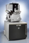
Hillsboro, OR | Posted on June 30th, 2013FEI will showcase its new Helios NanoLab™ 660 DualBeam™, at the upcoming Materials Research Society conference in Singapore. The Helios NanoLab 660 DualBeam system provides one of the highest imaging resolution and contrast SEMs, combined with one of the fastest and most precise FIB milling performances of any commercially-available focused ion beam/scanning electron microscope (FIB/SEM) system.
DualBeam (FIB/SEM) systems are used to investigate the structure and function of materials at the nanometer scale, create prototypes of micro and nano electro-mechanical systems (MEMS and NEMS), and prepare ultrathin samples for atomic scale imaging and analysis in a transmission electron microscope (TEM).
"The Helios NanoLab 660 DualBeam adds our second-generation extreme high-resolution (XHR) SEM capability to the proven Helios DualBeam platform to provide sub-nanometer imaging resolution over a wide range of accelerating voltages. Its precise selective contrast enhancement can be tailored to reveal the finest details of the sample's topography, structure, composition and more," said Trisha Rice, vice president and general manager, Materials Science Business Unit, FEI. "The combination of high-resolution, high-contrast imaging and high-performance milling allows researchers to access more accurate information from their sample in less time. A new high-current mode enables faster analysis."
"The Helios NanoLab DualBeam is indispensable for high-resolution imaging of surfaces, sections or volumes of a wide variety of materials, especially soft or delicate samples, such as carbon nanotubes, polymers, ceramics, catalysts, etc.," added Rice. "The SEM's exceptional performance at low accelerating voltages, reduces beam damage, and dramatically improves sensitivity to surface detail."
NanoBuilder™ 2.0, a second-generation nanoprototyping toolset now introduced on the Helios NanoLab 660, automatically fabricates 3D prototypes of nano- and microscale devices, such as nanosensors from computer-generated models, and thereby simplifies and accelerates the prototyping workflow. Starting with a CAD design, the NanoBuilder software directs FIB milling and deposition to build intricate 3D structures with features ranging in size from nanometers to millimeters.
FEI's second-generation XHR SEM uses proprietary electron optical and detector technologies to deliver sub-nanometer imaging resolution, with high signal collection efficiency and high contrast, over the widest range of accelerating voltages (0.5-30 kV). Fast time to data is enabled both by the new in-column detection, which allows simultaneous topographic and materials contrast imaging and precise materials information from triple backscattered electron filtering, and by the new high-current SEM mode, which delivers up to 100 nA in a micrometric spot. The Tomahawk™ FIB column guarantees the tightest beam at high and low currents, for fast, precise large-volume removal and polishing, respectively; and exceptional low-energy performance, to remove surface damage in the final polishing steps of thin sample preparation.
To optimally serve nanoprototyping and sample preparation applications, the Helios NanoLab 660 DualBeam continues to support FEI's latest technology advancements, such as the EasyLift™ nanomanipulator, for the fastest, most reliable thin sample preparation using the in situ lift out (INLO) method, and the MultiChem™ gas injector system, for gas-assisted etching and beam-induced deposition of materials with higher speed and quality, added flexibility and optimal process control.
For more information, please visit FEI at the 7th International Conference on Materials for Advanced Technologies, 30 June to 5 July, 2013, Suntec, Singapore.
####
About FEI Company
FEI (Nasdaq: FEIC) is a leading supplier of scientific instruments for nano-scale applications and solutions for industry and science. With more than 60 years of technological innovation and leadership, FEI has set the performance standard in transmission electron microscopes (TEM), scanning electron microscopes (SEM) and DualBeams™, which combine a SEM with a focused ion beam (FIB). FEI has over 2,500 employees and sales and service operations in more than 50 countries around the world. More information can be found at: www.fei.com.
FEI Safe Harbor Statement
This news release contains forward-looking statements that include statements regarding the performance capabilities and benefits of the Helios NanoLab 660 DualBeam system. Factors that could affect these forward-looking statements include but are not limited to failure of the product or technology to perform as expected and achieve anticipated results, unexpected technology problems and challenges, changes to the technology, the inability of FEI, its suppliers or project partners to make the technological advances required for the technology to achieve anticipated results, the inability of customers to develop and deploy the expected new applications and our ability to manufacture, ship and deliver the tools or software as expected. Please also refer to our Form 10-K, Forms 10-Q, Forms 8-K and other filings with the U.S. Securities and Exchange Commission for additional information on these factors and other factors that could cause actual results to differ materially from the forward-looking statements. FEI assumes no duty to update forward-looking statements.
For more information, please click here
Contacts:
Sandy Fewkes
MindWrite Communications, Inc.
408.224.4024 phone
408.529.9685 cell
www.mind-write.com
Copyright © FEI Company
If you have a comment, please Contact us.Issuers of news releases, not 7th Wave, Inc. or Nanotechnology Now, are solely responsible for the accuracy of the content.
Bookmark:


| Related News Press |
News and information
![]() Quantum computer improves AI predictions April 17th, 2026
Quantum computer improves AI predictions April 17th, 2026
![]() Flexible sensor gains sensitivity under pressure April 17th, 2026
Flexible sensor gains sensitivity under pressure April 17th, 2026
![]() A reusable chip for particulate matter sensing April 17th, 2026
A reusable chip for particulate matter sensing April 17th, 2026
![]() Detecting vibrational quantum beating in the predissociation dynamics of SF6 using time-resolved photoelectron spectroscopy April 17th, 2026
Detecting vibrational quantum beating in the predissociation dynamics of SF6 using time-resolved photoelectron spectroscopy April 17th, 2026
Imaging
![]() Simple algorithm paired with standard imaging tool could predict failure in lithium metal batteries August 8th, 2025
Simple algorithm paired with standard imaging tool could predict failure in lithium metal batteries August 8th, 2025
Announcements
![]() A fundamentally new therapeutic approach to cystic fibrosis: Nanobody repairs cellular defect April 17th, 2026
A fundamentally new therapeutic approach to cystic fibrosis: Nanobody repairs cellular defect April 17th, 2026
![]() UC Irvine physicists discover method to reverse ‘quantum scrambling’ : The work addresses the problem of information loss in quantum computing system April 17th, 2026
UC Irvine physicists discover method to reverse ‘quantum scrambling’ : The work addresses the problem of information loss in quantum computing system April 17th, 2026
Tools
![]() Metasurfaces smooth light to boost magnetic sensing precision January 30th, 2026
Metasurfaces smooth light to boost magnetic sensing precision January 30th, 2026
![]() From sensors to smart systems: the rise of AI-driven photonic noses January 30th, 2026
From sensors to smart systems: the rise of AI-driven photonic noses January 30th, 2026
![]() Japan launches fully domestically produced quantum computer: Expo visitors to experience quantum computing firsthand August 8th, 2025
Japan launches fully domestically produced quantum computer: Expo visitors to experience quantum computing firsthand August 8th, 2025
Events/Classes
![]() Institute for Nanoscience hosts annual proposal planning meeting May 16th, 2025
Institute for Nanoscience hosts annual proposal planning meeting May 16th, 2025
![]() A New Blue: Mysterious origin of the ribbontail ray’s electric blue spots revealed July 5th, 2024
A New Blue: Mysterious origin of the ribbontail ray’s electric blue spots revealed July 5th, 2024
![]() Researchers demonstrate co-propagation of quantum and classical signals: Study shows that quantum encryption can be implemented in existing fiber networks January 20th, 2023
Researchers demonstrate co-propagation of quantum and classical signals: Study shows that quantum encryption can be implemented in existing fiber networks January 20th, 2023
|
|
||
|
|
||
| The latest news from around the world, FREE | ||
|
|
||
|
|
||
| Premium Products | ||
|
|
||
|
Only the news you want to read!
Learn More |
||
|
|
||
|
Full-service, expert consulting
Learn More |
||
|
|
||