Home > Press > University of Illinois researchers measure near-field behavior of semiconductor plasmonic microparticles: Nanometer-scale heating reveals surface plasmon resonance
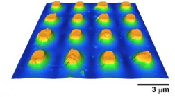 |
| Atomic force microscope image of plasmonic semiconductor microparticles. |
Abstract:
Recent progress in the engineering of plasmonic structures has enabled new kinds of nanometer-scale optoelectronic devices as well as high-resolution optical sensing. But until now, there has been a lack of tools for measuring nanometer-scale behavior in plasmonic structures which are needed to understand device performance and to confirm theoretical models.
University of Illinois researchers measure near-field behavior of semiconductor plasmonic microparticles: Nanometer-scale heating reveals surface plasmon resonance
Urbana, IL | Posted on April 22nd, 2013"For the first time, we have measured nanometer-scale infrared absorption in semiconductor plasmonic microparticles using a technique that combines atomic force microscopy with infrared spectroscopy," explained William P. King, an Abel Bliss Professor in the Department of Mechanical Science and Engineering (MechSE) at Illinois. "Atomic force microscope infrared spectroscopy allows us to directly observe the plasmonic behavior within microparticle infrared antennas."
The article describing the research, "Near-field infrared absorption of plasmonic semiconductor microparticles studied using atomic force microscope infrared spectroscopy," appears in Applied Physics Letters.
"Highly doped semiconductors can serve as wavelength flexible plasmonic metals in the infrared," noted Daniel M. Wasserman, assistant professor of electrical and computer engineering at Illinois. "However, without the ability to visualize the optical response in the vicinity of the plasmonic particles, we can only infer the near-field behavior of the structures from their far-field response. What this work gives us is a clear window into the optical behavior of this new class of materials on a length scale much smaller than the wavelength of light."
The article compares near-field and far-field measurements with electromagnetic simulations to confirm the presence of localized plasmonic resonance. The article further reports high resolution maps of the spatial distribution of absorption within single plasmonic structures and variation across plasmonic arrays.
"The ability to measure near field behavior in plasmonic structures allows us to begin expanding our design parameters for plasmonic materials," commented Jonathan Felts, a MechSE graduate student. "Now that we can measure the optical behavior of individual features, we can start to think about designing and testing more complex optical materials."
The authors on the research are Jonathan Felts, Stephanie Law, Daniel M. Wasserman, and William P. King of the University of Illinois at Urbana-Champaign, along with Christopher M. Roberts and Viktor Podolskiy of the University of Massachusetts. The article is available online. This research was supported by the National Science Foundation.
####
For more information, please click here
Contacts:
William P. King
217-244-3864
Copyright © University of Illinois College of Engineering
If you have a comment, please Contact us.Issuers of news releases, not 7th Wave, Inc. or Nanotechnology Now, are solely responsible for the accuracy of the content.
Bookmark:


| Related Links |
| Related News Press |
News and information
![]() Quantum computer improves AI predictions April 17th, 2026
Quantum computer improves AI predictions April 17th, 2026
![]() Flexible sensor gains sensitivity under pressure April 17th, 2026
Flexible sensor gains sensitivity under pressure April 17th, 2026
![]() A reusable chip for particulate matter sensing April 17th, 2026
A reusable chip for particulate matter sensing April 17th, 2026
![]() Detecting vibrational quantum beating in the predissociation dynamics of SF6 using time-resolved photoelectron spectroscopy April 17th, 2026
Detecting vibrational quantum beating in the predissociation dynamics of SF6 using time-resolved photoelectron spectroscopy April 17th, 2026
Imaging
![]() Simple algorithm paired with standard imaging tool could predict failure in lithium metal batteries August 8th, 2025
Simple algorithm paired with standard imaging tool could predict failure in lithium metal batteries August 8th, 2025
Govt.-Legislation/Regulation/Funding/Policy
![]() Quantum computer improves AI predictions April 17th, 2026
Quantum computer improves AI predictions April 17th, 2026
![]() Metasurfaces smooth light to boost magnetic sensing precision January 30th, 2026
Metasurfaces smooth light to boost magnetic sensing precision January 30th, 2026
![]() New imaging approach transforms study of bacterial biofilms August 8th, 2025
New imaging approach transforms study of bacterial biofilms August 8th, 2025
Chip Technology
![]() A reusable chip for particulate matter sensing April 17th, 2026
A reusable chip for particulate matter sensing April 17th, 2026
![]() Metasurfaces smooth light to boost magnetic sensing precision January 30th, 2026
Metasurfaces smooth light to boost magnetic sensing precision January 30th, 2026
Optical computing/Photonic computing
![]() ICFO researchers overcome long-standing bottleneck in single photon detection with twisted 2D materials August 8th, 2025
ICFO researchers overcome long-standing bottleneck in single photon detection with twisted 2D materials August 8th, 2025
![]() Programmable electron-induced color router array May 14th, 2025
Programmable electron-induced color router array May 14th, 2025
Discoveries
![]() Quantum computer improves AI predictions April 17th, 2026
Quantum computer improves AI predictions April 17th, 2026
![]() Flexible sensor gains sensitivity under pressure April 17th, 2026
Flexible sensor gains sensitivity under pressure April 17th, 2026
![]() A reusable chip for particulate matter sensing April 17th, 2026
A reusable chip for particulate matter sensing April 17th, 2026
![]() Detecting vibrational quantum beating in the predissociation dynamics of SF6 using time-resolved photoelectron spectroscopy April 17th, 2026
Detecting vibrational quantum beating in the predissociation dynamics of SF6 using time-resolved photoelectron spectroscopy April 17th, 2026
Announcements
![]() A fundamentally new therapeutic approach to cystic fibrosis: Nanobody repairs cellular defect April 17th, 2026
A fundamentally new therapeutic approach to cystic fibrosis: Nanobody repairs cellular defect April 17th, 2026
![]() UC Irvine physicists discover method to reverse �quantum scrambling� : The work addresses the problem of information loss in quantum computing system April 17th, 2026
UC Irvine physicists discover method to reverse �quantum scrambling� : The work addresses the problem of information loss in quantum computing system April 17th, 2026
Interviews/Book Reviews/Essays/Reports/Podcasts/Journals/White papers/Posters
![]() A fundamentally new therapeutic approach to cystic fibrosis: Nanobody repairs cellular defect April 17th, 2026
A fundamentally new therapeutic approach to cystic fibrosis: Nanobody repairs cellular defect April 17th, 2026
![]() UC Irvine physicists discover method to reverse �quantum scrambling� : The work addresses the problem of information loss in quantum computing system April 17th, 2026
UC Irvine physicists discover method to reverse �quantum scrambling� : The work addresses the problem of information loss in quantum computing system April 17th, 2026
Tools
![]() Metasurfaces smooth light to boost magnetic sensing precision January 30th, 2026
Metasurfaces smooth light to boost magnetic sensing precision January 30th, 2026
![]() From sensors to smart systems: the rise of AI-driven photonic noses January 30th, 2026
From sensors to smart systems: the rise of AI-driven photonic noses January 30th, 2026
![]() Japan launches fully domestically produced quantum computer: Expo visitors to experience quantum computing firsthand August 8th, 2025
Japan launches fully domestically produced quantum computer: Expo visitors to experience quantum computing firsthand August 8th, 2025
Photonics/Optics/Lasers
![]() Metasurfaces smooth light to boost magnetic sensing precision January 30th, 2026
Metasurfaces smooth light to boost magnetic sensing precision January 30th, 2026
![]() From sensors to smart systems: the rise of AI-driven photonic noses January 30th, 2026
From sensors to smart systems: the rise of AI-driven photonic noses January 30th, 2026
Research partnerships
![]() Lab to industry: InSe wafer-scale breakthrough for future electronics August 8th, 2025
Lab to industry: InSe wafer-scale breakthrough for future electronics August 8th, 2025
![]() HKU physicists uncover hidden order in the quantum world through deconfined quantum critical points April 25th, 2025
HKU physicists uncover hidden order in the quantum world through deconfined quantum critical points April 25th, 2025
|
|
||
|
|
||
| The latest news from around the world, FREE | ||
|
|
||
|
|
||
| Premium Products | ||
|
|
||
|
Only the news you want to read!
Learn More |
||
|
|
||
|
Full-service, expert consulting
Learn More |
||
|
|
||