Home > Press > High-performance, NW-OPTs open the way for optoelectronic device miniaturization
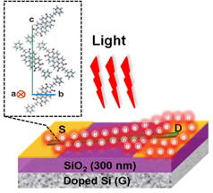 |
| Schematic diagram of single-crystalline nanowire organic phototransistors
Copyright @ Wiley-VCH Verlag GmbH & Co. KGaA. |
Abstract:
Research team of Ulsan National Institute of Science and Technology (UNIST), Ulsan, South Korea, developed high-performance organic phototransistors (OPTs) based on single-crystalline n-channel organic nanowires.
High-performance, NW-OPTs open the way for optoelectronic device miniaturization
Ulsan, Republic of Korea | Posted on March 12th, 2013 Phototransistors are a kind of transistors in which the incident light intensity can modulate the charge-carrier density in the channel. Compared with conventional photodiodes, phototransistors enable easier control of light-detection sensitivity without problems such as the noise increment. However, to date, the research has mostly focused on thin-film OPTs, and nanoscale OPTs have scarcely been reported.
OPTs have many intrinsic advantages over their inorganic counterparts, such as the chemical tunability of optoelectronic properties by molecular design and high potential in low cost, light-weight, flexible applications.
Single-crystalline nano-/microwires (NWs/MWs) based on organic semiconductors have attracted great interest recently as they are promising building blocks for various electronic and optoelectronic applications. In particular, OPTs based on single-crystalline NWs/MWs may yield higher light sensitivity than their bulk counterparts. In addition, their one-dimensional, intrinsically defect-free and highly ordered nature will allow a deeper understanding of the fundamental mechanisms of charge generation and transport in OPTs, while enabling a bottom-up fabrication of optoelectronic nanodevices.
Prof. Joon Hak Oh and Hojeong Yu, working at UNIST, together with Prof. Zhenan Bao at Stanford University, USA, have worked on n-channel single-crystalline nanowire organic phototransistors (NW-OPTs) and observed significant enhancement in the charge-carrier mobility of NW-OPTs.
Prof. Oh said, "The development of OPTs based on n-channel single-crystalline organic semiconducting NWs/MWs is highly desirable for the bottom-up fabrication of complementary metal oxide semiconductor (CMOS)-like photoelectronic circuits, which provides various advantages such as high operational stability, easy control of photoswitching voltages, high photosensitivity and responsivity."
The photoelectronic characteristics of the single-crystalline NW-OPTs such as the photoresponsivity, the photo-switching ratio, and the photoconductive gain, were analyzed from the I-V characteristics coupled with light irradiation and compared with those of vacuum-deposited thin-film devices. The external quantum efficiencies (EQEs) were also investigated for the NW-OPTs and thin-film OPTs. In addition, they calculated the charge accumulation and release rates from deep traps, and investigated the effects of incident light intensity on their photoelectronic properties.
A mobility enhancement is observed when the incident optical power density increases and the wavelength of the light source matches the light-absorption range of the photoactive material. The photoswitching ratio is strongly dependent upon the incident optical power density, whereas the photoresponsivity is more dependent on matching the light-source wavelength with the maximum absorption range of the photoactive material.
NW-OPTs based on n-channel semiconductor, N,N ′-bis(2-phenylethyl)-perylene-3,4:9,10-tetracarboxylic diimide (BPE-PTCDI), exhibited much higher external quantum efficiency (EQE) values (≈7900 times larger) than thin-film OPTs, with a maximum EQE of 263 000%. This phenomena result from the intrinsically defect-free single-crystalline nature of the BPE-PTCDI NWs. In addition, an approach was devised to analyze the charge-transport behaviors using charge accumulation/release rates from deep traps under on/off switching of external light sources.
"Our approach to charge-accumulation/release-rate calculations could provide a fundamental understanding about charge-carrier-density variations under light irradiation, which subsequently enables in-depth study of OPTs," said Prof. Oh, "Hence organic single-crystalline NW-OPTs are a highly promising alternative to conventional thin-film-type photodiodes, and can effectively pave the way for optoelectronic device miniaturization."
This research was supported by a National Research Foundation of Korea (NRF) Grant funded by the Ministry of Education, Science, and Technology (MEST), and the Global Frontier Research Center for Advanced Soft Electronics and published in Advanced Functional Materials (Title: High-Performance Phototransistors Based on Single-Crystalline n-Channel Organic Nanowires and Photogenerated Charge-Carrier Behaviors, 5 Feb 2013).
####
For more information, please click here
Contacts:
Eunhee Song
82-522-171-224
Copyright © Ulsan National Institute of Science and Technology
If you have a comment, please Contact us.Issuers of news releases, not 7th Wave, Inc. or Nanotechnology Now, are solely responsible for the accuracy of the content.
Bookmark:


| Related Links |
| Related News Press |
News and information
![]() Simulating magnetization in a Heisenberg quantum spin chain April 5th, 2024
Simulating magnetization in a Heisenberg quantum spin chain April 5th, 2024
![]() NRL charters Navy�s quantum inertial navigation path to reduce drift April 5th, 2024
NRL charters Navy�s quantum inertial navigation path to reduce drift April 5th, 2024
![]() Discovery points path to flash-like memory for storing qubits: Rice find could hasten development of nonvolatile quantum memory April 5th, 2024
Discovery points path to flash-like memory for storing qubits: Rice find could hasten development of nonvolatile quantum memory April 5th, 2024
Govt.-Legislation/Regulation/Funding/Policy
![]() NRL charters Navy�s quantum inertial navigation path to reduce drift April 5th, 2024
NRL charters Navy�s quantum inertial navigation path to reduce drift April 5th, 2024
![]() Discovery points path to flash-like memory for storing qubits: Rice find could hasten development of nonvolatile quantum memory April 5th, 2024
Discovery points path to flash-like memory for storing qubits: Rice find could hasten development of nonvolatile quantum memory April 5th, 2024
![]() Chemical reactions can scramble quantum information as well as black holes April 5th, 2024
Chemical reactions can scramble quantum information as well as black holes April 5th, 2024
Chip Technology
![]() Discovery points path to flash-like memory for storing qubits: Rice find could hasten development of nonvolatile quantum memory April 5th, 2024
Discovery points path to flash-like memory for storing qubits: Rice find could hasten development of nonvolatile quantum memory April 5th, 2024
![]() Utilizing palladium for addressing contact issues of buried oxide thin film transistors April 5th, 2024
Utilizing palladium for addressing contact issues of buried oxide thin film transistors April 5th, 2024
![]() HKUST researchers develop new integration technique for efficient coupling of III-V and silicon February 16th, 2024
HKUST researchers develop new integration technique for efficient coupling of III-V and silicon February 16th, 2024
Discoveries
![]() Chemical reactions can scramble quantum information as well as black holes April 5th, 2024
Chemical reactions can scramble quantum information as well as black holes April 5th, 2024
![]() New micromaterial releases nanoparticles that selectively destroy cancer cells April 5th, 2024
New micromaterial releases nanoparticles that selectively destroy cancer cells April 5th, 2024
![]() Utilizing palladium for addressing contact issues of buried oxide thin film transistors April 5th, 2024
Utilizing palladium for addressing contact issues of buried oxide thin film transistors April 5th, 2024
Announcements
![]() NRL charters Navy�s quantum inertial navigation path to reduce drift April 5th, 2024
NRL charters Navy�s quantum inertial navigation path to reduce drift April 5th, 2024
![]() Discovery points path to flash-like memory for storing qubits: Rice find could hasten development of nonvolatile quantum memory April 5th, 2024
Discovery points path to flash-like memory for storing qubits: Rice find could hasten development of nonvolatile quantum memory April 5th, 2024
Photonics/Optics/Lasers
![]() With VECSELs towards the quantum internet Fraunhofer: IAF achieves record output power with VECSEL for quantum frequency converters April 5th, 2024
With VECSELs towards the quantum internet Fraunhofer: IAF achieves record output power with VECSEL for quantum frequency converters April 5th, 2024
![]() Nanoscale CL thermometry with lanthanide-doped heavy-metal oxide in TEM March 8th, 2024
Nanoscale CL thermometry with lanthanide-doped heavy-metal oxide in TEM March 8th, 2024
![]() Optically trapped quantum droplets of light can bind together to form macroscopic complexes March 8th, 2024
Optically trapped quantum droplets of light can bind together to form macroscopic complexes March 8th, 2024
![]() HKUST researchers develop new integration technique for efficient coupling of III-V and silicon February 16th, 2024
HKUST researchers develop new integration technique for efficient coupling of III-V and silicon February 16th, 2024
Research partnerships
![]() Discovery points path to flash-like memory for storing qubits: Rice find could hasten development of nonvolatile quantum memory April 5th, 2024
Discovery points path to flash-like memory for storing qubits: Rice find could hasten development of nonvolatile quantum memory April 5th, 2024
![]() Researchers� approach may protect quantum computers from attacks March 8th, 2024
Researchers� approach may protect quantum computers from attacks March 8th, 2024
![]() 'Sudden death' of quantum fluctuations defies current theories of superconductivity: Study challenges the conventional wisdom of superconducting quantum transitions January 12th, 2024
'Sudden death' of quantum fluctuations defies current theories of superconductivity: Study challenges the conventional wisdom of superconducting quantum transitions January 12th, 2024
|
|
||
|
|
||
| The latest news from around the world, FREE | ||
|
|
||
|
|
||
| Premium Products | ||
|
|
||
|
Only the news you want to read!
Learn More |
||
|
|
||
|
Full-service, expert consulting
Learn More |
||
|
|
||