Home > Press > New player in electron field emitter technology makes for better imaging and communications
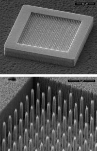 |
| NIST's silicon carbide field emitter produces a flow of electrons comparable to hot sources, but without the need for heat. By dissolving much of the material away to make a porous structure with a large surface area, NIST scientists ensured that as an electron emission point on an individual spike wears out, another is available to take its place, making the array more durable as a whole.
Credit: Sharifi/NIST |
Abstract:
Scientists at the National Institute of Standards and Technology (NIST) and the University of Maryland, College Park, have built a practical, high-efficiency nanostructured electron source. Described in the journal Nanotechnology*, this new, patent-pending technology could lead to improved microwave communications and radar, and more notably to new and improved X-ray imaging systems for security and health-care applications.
New player in electron field emitter technology makes for better imaging and communications
Gaithersburg, MD | Posted on March 9th, 2013While thermionic electron sources such as the hot filaments inside cathode ray tubes have largely been replaced by LEDs and liquid crystals for display screens and televisions, they are still used to produce microwaves for radar and X-rays for medical imaging. Thermionic sources use an electric current to boil electrons off the surface of a wire filament, similar to the way an incandescent light bulb uses an electric current to heat a wire filament until it glows.
And like an incandescent light bulb, thermionic sources are generally not very energy efficient. It takes a lot of power to boil off the electrons, which spew in every direction. Those that aren't lost have to be captured and focused using a complicated system of electric and magnetic fields. Field emission electron sources require much less power and produce a much more directional and easily controllable stream of electrons.
To build their field emission source, the NIST team took a tough material�silicon carbide�and used a room-temperature chemical process to make it highly porous like a sponge. They then patterned it into microscopic emitting structures in the shape of pointed rods or sharp-edged fins. When an electric field is applied, these novel field emitters can produce an electron flow comparable to a thermionic source but without all the disadvantages�and with many advantages.
According to co-inventor Fred Sharifi, the new field emitters have inherently fast response times compared with thermionic sources, and the absence of heat makes it easier to create arrays of sources. Moreover, the porous nanostructure of the emitters makes them very reliable. Even if the emitter surface wears away during use�a common problem�the newly exposed material continues to work just as well.
Sharifi says that the NIST field emitters hold the potential to enhance the resolution and quality of X-ray images and allow for new modes of detection.
"X-ray images are based on the density of the material being examined, which limits their ability to see certain types of materials, including some types of explosives," says Sharifi. "Our field emitter will let us see not just that something is there, but, because we can build large arrays and place them at different angles, we can identify the material in question by looking at how the X-rays coming from different directions scatter from the object."
The technology is available for licensing through NIST's Technology Partnerships Office.
*M. Kang, H. Lezec and F. Sharifi. Stable field emission from nanoporous silicon carbide. Nanotechnology. 24 (2013) 065201.
####
For more information, please click here
Contacts:
Mark Esser
301-975-8735
Copyright © National Institute of Standards and Technology (NIST)
If you have a comment, please Contact us.Issuers of news releases, not 7th Wave, Inc. or Nanotechnology Now, are solely responsible for the accuracy of the content.
Bookmark:


| Related News Press |
News and information
![]() Quantum computer improves AI predictions April 17th, 2026
Quantum computer improves AI predictions April 17th, 2026
![]() Flexible sensor gains sensitivity under pressure April 17th, 2026
Flexible sensor gains sensitivity under pressure April 17th, 2026
![]() A reusable chip for particulate matter sensing April 17th, 2026
A reusable chip for particulate matter sensing April 17th, 2026
![]() Detecting vibrational quantum beating in the predissociation dynamics of SF6 using time-resolved photoelectron spectroscopy April 17th, 2026
Detecting vibrational quantum beating in the predissociation dynamics of SF6 using time-resolved photoelectron spectroscopy April 17th, 2026
Imaging
![]() Simple algorithm paired with standard imaging tool could predict failure in lithium metal batteries August 8th, 2025
Simple algorithm paired with standard imaging tool could predict failure in lithium metal batteries August 8th, 2025
![]() First real-time observation of two-dimensional melting process: Researchers at Mainz University unveil new insights into magnetic vortex structures August 8th, 2025
First real-time observation of two-dimensional melting process: Researchers at Mainz University unveil new insights into magnetic vortex structures August 8th, 2025
![]() New imaging approach transforms study of bacterial biofilms August 8th, 2025
New imaging approach transforms study of bacterial biofilms August 8th, 2025
Laboratories
![]() Researchers develop molecular qubits that communicate at telecom frequencies October 3rd, 2025
Researchers develop molecular qubits that communicate at telecom frequencies October 3rd, 2025
Govt.-Legislation/Regulation/Funding/Policy
![]() Quantum computer improves AI predictions April 17th, 2026
Quantum computer improves AI predictions April 17th, 2026
![]() Metasurfaces smooth light to boost magnetic sensing precision January 30th, 2026
Metasurfaces smooth light to boost magnetic sensing precision January 30th, 2026
![]() New imaging approach transforms study of bacterial biofilms August 8th, 2025
New imaging approach transforms study of bacterial biofilms August 8th, 2025
Discoveries
![]() Quantum computer improves AI predictions April 17th, 2026
Quantum computer improves AI predictions April 17th, 2026
![]() Flexible sensor gains sensitivity under pressure April 17th, 2026
Flexible sensor gains sensitivity under pressure April 17th, 2026
![]() A reusable chip for particulate matter sensing April 17th, 2026
A reusable chip for particulate matter sensing April 17th, 2026
![]() Detecting vibrational quantum beating in the predissociation dynamics of SF6 using time-resolved photoelectron spectroscopy April 17th, 2026
Detecting vibrational quantum beating in the predissociation dynamics of SF6 using time-resolved photoelectron spectroscopy April 17th, 2026
Announcements
![]() A fundamentally new therapeutic approach to cystic fibrosis: Nanobody repairs cellular defect April 17th, 2026
A fundamentally new therapeutic approach to cystic fibrosis: Nanobody repairs cellular defect April 17th, 2026
![]() UC Irvine physicists discover method to reverse �quantum scrambling� : The work addresses the problem of information loss in quantum computing system April 17th, 2026
UC Irvine physicists discover method to reverse �quantum scrambling� : The work addresses the problem of information loss in quantum computing system April 17th, 2026
Patents/IP/Tech Transfer/Licensing
![]() Getting drugs across the blood-brain barrier using nanoparticles March 3rd, 2023
Getting drugs across the blood-brain barrier using nanoparticles March 3rd, 2023
![]() Metasurfaces control polarized light at will: New research unlocks the hidden potential of metasurfaces August 13th, 2021
Metasurfaces control polarized light at will: New research unlocks the hidden potential of metasurfaces August 13th, 2021
![]() Arrowhead Pharmaceuticals Announces Closing of Agreement with Takeda November 27th, 2020
Arrowhead Pharmaceuticals Announces Closing of Agreement with Takeda November 27th, 2020
Research partnerships
![]() Lab to industry: InSe wafer-scale breakthrough for future electronics August 8th, 2025
Lab to industry: InSe wafer-scale breakthrough for future electronics August 8th, 2025
![]() HKU physicists uncover hidden order in the quantum world through deconfined quantum critical points April 25th, 2025
HKU physicists uncover hidden order in the quantum world through deconfined quantum critical points April 25th, 2025
|
|
||
|
|
||
| The latest news from around the world, FREE | ||
|
|
||
|
|
||
| Premium Products | ||
|
|
||
|
Only the news you want to read!
Learn More |
||
|
|
||
|
Full-service, expert consulting
Learn More |
||
|
|
||