Home > Press > ‘Slow Light’ Advance Could Speed Optical Computing, Telecommunications: Metamaterials provide active control of slow-light devices
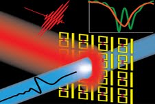 |
| Schematic of active optical control of terahertz waves in electromagnetically induced transparency metamaterials. |
Abstract:
Wireless communications and optical computing could soon get a significant boost in speed, thanks to "slow light" and specialized metamaterials through which it travels.
‘Slow Light’ Advance Could Speed Optical Computing, Telecommunications: Metamaterials provide active control of slow-light devices
Los Alamos, NM | Posted on February 12th, 2013Researchers have made the first demonstration of rapidly switching on and off "slow light" in specially designed materials at room temperature. This work opens the possibility to design novel, chip-scale, ultrafast devices for applications in terahertz wireless communications and all-optical computing.
Significance of the research
In slow light, a propagating light pulse is substantially slowed down, compared with the velocity of light in a vacuum. This is accomplished by the light's interaction with the medium through which it is shining. Slow light has potential applications in telecommunications because it could lead to a more orderly traffic flow in networks.
Like cars slowing down or speeding up to negotiate an intersection, packets of information are better managed if their transmission speed is changeable. Another potential application is the storage of information carried by light pulses, leading to a potential all-optical computing system. Current semiconductor materials used in computing devices are reaching some of their limits, and an all-optical system would potentially enable improvements in size reduction and calculation speeds.
The effects of strong light-matter coupling used in slowing down light might create entangled photon pairs that lead to quantum computing capabilities beyond those of modern computers, the researchers say.
Giving classical optical structures a quantum twist
Electromagnetically induced transparency is a quantum interference effect that produces a sharp resonance with extremely low loss and dispersion. However, implementing electromagnetically induced transparency in chip-scale applications is difficult due to the demands of stable gas lasers and low-temperature environments. The key to success is the use of metamaterials, engineered artificial materials containing structures that are smaller than the wavelength of the waves they affect.
Researchers integrated photoconductive silicon into the metamaterial unit cell. This material enables a switching of the transparency resonance window through the excitation of ultrafast, femto-second optical pulses. This phenomenon causes an optically tunable group delay of the terahertz light. The "slow light" behavior can be controlled at an ultrafast time scale by integrating appropriate semiconductor materials with conventional metamaterial designs.
In this research, the medium is an active metamaterial that supports a sharp resonance, which leads to a rapid change in the refractive index of the medium over a small range of frequencies. This phenomenon causes a dramatic reduction in the velocity of terahertz light propagation. The resonance can be switched on and off on a time scale of a few pico-seconds. When the resonance transparency is on, the system produces slow light. When the resonance is off, the slow light behavior disappears. This on and off process happens on an ultrafast (pico-second) time scale when a femto-second laser pulse excites the metamaterial. Nature Communications published the research.
The research team
Researchers include Ranjan Singh of High Power Electrodynamics, Abdul K. Azad and Hou-Tong Chen of the Center for Integrated Nanotechnologies, Antoinette Taylor of Materials Physics and Applications, collaborators from Tianjin University, Oklahoma State University, and Imperial College, London. The U.S. Department of Energy supported the LANL research, which was performed, in part, at the Center for Integrated Nanotechnologies, a DOE Office of Science user facility. The work supports the Laboratory's global- and energy-security mission areas.
Additional information
Slow light is just that, light that has been slowed from the traditionally understood standard, 299,792,458 meters per second. While faster-than-light speeds are considered impossible, it is entirely reasonable to guide light through a material that slows or delays the motion of the photons as they move through the medium. The photons are absorbed and then re-emitted, slowing the transmission from one area to another, and in some experiments the light has been stopped altogether. The measurement of how much light is slowed in a material is known as its refractive index. In a vacuum, there is no delay. Through a diamond, with a refractive index of 2.4, the light lingers for a small time.
Metamaterials are assemblies of multiple individual elements fashioned from conventional microscopic materials arranged in periodic patterns. The precise shape, geometry, size, orientation and arrangement of the structures can affect waves of light in an unconventional manner, creating material properties that are unachievable with conventional materials.
####
About Los Alamos National Laboratory
Los Alamos National Laboratory, a multidisciplinary research institution engaged in strategic science on behalf of national security, is operated by Los Alamos National Security, LLC, a team composed of Bechtel National, the University of California, The Babcock & Wilcox Company, and URS for the Department of Energy’s National Nuclear Security Administration.
Los Alamos enhances national security by ensuring the safety and reliability of the U.S. nuclear stockpile, developing technologies to reduce threats from weapons of mass destruction, and solving problems related to energy, environment, infrastructure, health, and global security concerns.
About the Center for Integrated Nanotechnologies
The Center for Nanoscale Materials is one of the five DOE Nanoscale Science Research Centers, premier national user facilities for interdisciplinary research at the nanoscale supported by the U.S. Department of Energy, Office of Science. Together the NSRCs comprise a suite of complementary facilities that provide researchers with state-of-the-art capabilities to fabricate, process, characterize and model nanoscale materials, and constitute the largest infrastructure investment of the National Nanotechnology Initiative. The NSRCs are located at DOE's Argonne, Brookhaven, Lawrence Berkeley, Oak Ridge, Sandia and Los Alamos National Laboratories. For more information about the DOE NSRCs, please click here.
For more information, please click here
Contacts:
Nancy Ambrosiano
505.667.0471
Copyright © Los Alamos National Laboratory
If you have a comment, please Contact us.Issuers of news releases, not 7th Wave, Inc. or Nanotechnology Now, are solely responsible for the accuracy of the content.
Bookmark:


| Related Links |
| Related News Press |
News and information
![]() Quantum computer improves AI predictions April 17th, 2026
Quantum computer improves AI predictions April 17th, 2026
![]() Flexible sensor gains sensitivity under pressure April 17th, 2026
Flexible sensor gains sensitivity under pressure April 17th, 2026
![]() A reusable chip for particulate matter sensing April 17th, 2026
A reusable chip for particulate matter sensing April 17th, 2026
![]() Detecting vibrational quantum beating in the predissociation dynamics of SF6 using time-resolved photoelectron spectroscopy April 17th, 2026
Detecting vibrational quantum beating in the predissociation dynamics of SF6 using time-resolved photoelectron spectroscopy April 17th, 2026
Laboratories
![]() Researchers develop molecular qubits that communicate at telecom frequencies October 3rd, 2025
Researchers develop molecular qubits that communicate at telecom frequencies October 3rd, 2025
![]() A battery’s hopping ions remember where they’ve been: Seen in atomic detail, the seemingly smooth flow of ions through a battery’s electrolyte is surprisingly complicated February 16th, 2024
A battery’s hopping ions remember where they’ve been: Seen in atomic detail, the seemingly smooth flow of ions through a battery’s electrolyte is surprisingly complicated February 16th, 2024
Govt.-Legislation/Regulation/Funding/Policy
![]() Quantum computer improves AI predictions April 17th, 2026
Quantum computer improves AI predictions April 17th, 2026
![]() Metasurfaces smooth light to boost magnetic sensing precision January 30th, 2026
Metasurfaces smooth light to boost magnetic sensing precision January 30th, 2026
![]() New imaging approach transforms study of bacterial biofilms August 8th, 2025
New imaging approach transforms study of bacterial biofilms August 8th, 2025
Optical computing/Photonic computing
![]() ICFO researchers overcome long-standing bottleneck in single photon detection with twisted 2D materials August 8th, 2025
ICFO researchers overcome long-standing bottleneck in single photon detection with twisted 2D materials August 8th, 2025
![]() Programmable electron-induced color router array May 14th, 2025
Programmable electron-induced color router array May 14th, 2025
Materials/Metamaterials/Magnetoresistance
![]() First real-time observation of two-dimensional melting process: Researchers at Mainz University unveil new insights into magnetic vortex structures August 8th, 2025
First real-time observation of two-dimensional melting process: Researchers at Mainz University unveil new insights into magnetic vortex structures August 8th, 2025
![]() Researchers unveil a groundbreaking clay-based solution to capture carbon dioxide and combat climate change June 6th, 2025
Researchers unveil a groundbreaking clay-based solution to capture carbon dioxide and combat climate change June 6th, 2025
![]() A 1960s idea inspires NBI researchers to study hitherto inaccessible quantum states June 6th, 2025
A 1960s idea inspires NBI researchers to study hitherto inaccessible quantum states June 6th, 2025
![]() Institute for Nanoscience hosts annual proposal planning meeting May 16th, 2025
Institute for Nanoscience hosts annual proposal planning meeting May 16th, 2025
Announcements
![]() A fundamentally new therapeutic approach to cystic fibrosis: Nanobody repairs cellular defect April 17th, 2026
A fundamentally new therapeutic approach to cystic fibrosis: Nanobody repairs cellular defect April 17th, 2026
![]() UC Irvine physicists discover method to reverse ‘quantum scrambling’ : The work addresses the problem of information loss in quantum computing system April 17th, 2026
UC Irvine physicists discover method to reverse ‘quantum scrambling’ : The work addresses the problem of information loss in quantum computing system April 17th, 2026
Photonics/Optics/Lasers
![]() Metasurfaces smooth light to boost magnetic sensing precision January 30th, 2026
Metasurfaces smooth light to boost magnetic sensing precision January 30th, 2026
![]() From sensors to smart systems: the rise of AI-driven photonic noses January 30th, 2026
From sensors to smart systems: the rise of AI-driven photonic noses January 30th, 2026
|
|
||
|
|
||
| The latest news from around the world, FREE | ||
|
|
||
|
|
||
| Premium Products | ||
|
|
||
|
Only the news you want to read!
Learn More |
||
|
|
||
|
Full-service, expert consulting
Learn More |
||
|
|
||