Home > Press > 3D Printing on the Micrometer Scale: KIT Spin-off “Nanoscribe“ Presents High-speed 3D Printer
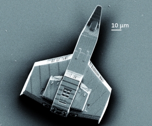 |
| Printing on the micrometer scale: Writing time for a miniaturized spacecraft is reduced to less than one minute without loss of quality. (Photo: Nanoscribe) |
Abstract:
At the Photonics West, the leading international fair for photonics taking place in San Francisco (USA) this week, Nanoscribe GmbH, a spin-off of Karlsruhe Institute of Technology (KIT), presents the world's fastest 3D printer of micro- and nanostructures. With this printer, smallest three-dimensional objects, often smaller than the diameter of a human hair, can be manufactured with minimum time consumption and maximum resolution. The printer is based on a novel laser lithography method.
3D Printing on the Micrometer Scale: KIT Spin-off “Nanoscribe“ Presents High-speed 3D Printer
Germany | Posted on February 8th, 2013 "The success of Nanoscribe is an example of KIT's excellent entrepreneurial culture and confirms our strategy of specifically supporting spin-offs. In this way, research results are transferred rapidly and sustainably to the market," says Dr. Peter Fritz, KIT Vice President for Research and Innovation. In early 2008, Nanoscribe was founded as the first spin-off of KIT and has since established itself as the world's market and technology leader in the area of 3D laser lithography.
Last year, 18 spin-offs were established at KIT. The 3D laser litho-graphy systems developed by Nanoscribe - the spin-off can still be found on KIT's Campus North - are used for research by KIT and scientists worldwide. Work in the area of photonics concentrates on replacing conventional electronics by optical circuits of higher performance. For this purpose, Nanoscribe systems are used to print polymer waveguides reaching data transfer rates of more than 5 terabits per second.
Biosciences produce tailored scaffolds for cell growth studies among others. In materials research, functional materials of enhanced performance are developed for lightweight construction to reduce the consumption of resources. Among the customers are universities and research institutions as well as industrial companies.
Increased Speed: Hours Turn into Minutes
By means of the new laser lithography method, printing speed is increased by factor of about 100. This increase in speed results from the use of a galvo mirror system, a technology that is also applied in laser show devices or scanning units of CD and DVD drives. Reflecting a laser beam off the rotating galvo mirrors facilitates rapid and precise laser focus positioning. "We are revolutionizing 3D printing on the micrometer scale. Precision and speed are achieved by the industrially established galvo technology. Our product benefits from more than one decade of experience in photonics, the key technology of the 21st century," says Martin Hermatschweiler, the managing director of Nanoscribe GmbH.
Mechanism: Two-photon Polymerization
The direct laser writing technique underlying the 3D printing method is based on two-photon polymerization. Just as paper ignites when exposed to sunlight focused through a magnifying glass, ultra-short laser pulses polymerize photosensitive materials in the laser focus. Depending on the photosensitive material chosen, the exposed or unexposed volume only is dissolved. After a developer bath, these written areas remain as self-supporting micro- and nanostructures.
Removing Barriers
By means of the galvo technology, three-dimensional micro- and nanostructures can be printed rapidly and, hence, on large areas in principle. At highest resolution, however, the scanning field is limited physically to a few 100 µm due to the optical properties of the focusing objective. Just as floor tiles must be joined precisely, the respective scanning fields have to be connected seamlessly and accurately. By the so-called stitching, areas can be extended nearly arbitrarily.
####
About Karlsruhe Institute of Technology (KIT)
Karlsruhe Institute of Technology (KIT) is a public corporation according to the legislation of the state of Baden-Württemberg. It fulfills the mission of a university and the mission of a national research center of the Helmholtz Association. KIT focuses on a knowledge triangle that links the tasks of research, teaching, and innovation.
About Nanoscribe
In early 2008, Nanoscribe GmbH was founded as the first spin-off of Karlsruhe Institute of Technology (KIT). Within a period of five years, it has established itself as the world’s market and technology leader in the area of 3D laser lithography. The devices produced by Nanoscribe are applied by leading research institutes and universities in Asia, North America, and Europe. Research into this technology has given rise to more than 60 scientific publications in high-ranking science journals and expert media.
www.nanoscribe.de
For more information, please click here
Contacts:
Monika Landgraf
49-721-608-47414
Nanoscribe GmbH
Anke Werner
Tel.: +49 721 608-28849
Fax.: +49 721 608-28848
werner∂nanoscribe de
Copyright © Karlsruhe Institute of Technology (KIT)
If you have a comment, please Contact us.Issuers of news releases, not 7th Wave, Inc. or Nanotechnology Now, are solely responsible for the accuracy of the content.
Bookmark:


| Related News Press |
News and information
![]() Quantum computer improves AI predictions April 17th, 2026
Quantum computer improves AI predictions April 17th, 2026
![]() Flexible sensor gains sensitivity under pressure April 17th, 2026
Flexible sensor gains sensitivity under pressure April 17th, 2026
![]() A reusable chip for particulate matter sensing April 17th, 2026
A reusable chip for particulate matter sensing April 17th, 2026
![]() Detecting vibrational quantum beating in the predissociation dynamics of SF6 using time-resolved photoelectron spectroscopy April 17th, 2026
Detecting vibrational quantum beating in the predissociation dynamics of SF6 using time-resolved photoelectron spectroscopy April 17th, 2026
3D & 4D printing/Additive-manufacturing
![]() Presenting: Ultrasound-based printing of 3D materials—potentially inside the body December 8th, 2023
Presenting: Ultrasound-based printing of 3D materials—potentially inside the body December 8th, 2023
![]() Fiber sensing scientists invent 3D printed fiber microprobe for measuring in vivo biomechanical properties of tissue and even single cell February 10th, 2023
Fiber sensing scientists invent 3D printed fiber microprobe for measuring in vivo biomechanical properties of tissue and even single cell February 10th, 2023
![]() 3D-printed decoder, AI-enabled image compression could enable higher-res displays December 9th, 2022
3D-printed decoder, AI-enabled image compression could enable higher-res displays December 9th, 2022
![]() Researchers design new inks for 3D-printable wearable bioelectronics: Potential uses include printing electronic tattoos for medical tracking applications August 19th, 2022
Researchers design new inks for 3D-printable wearable bioelectronics: Potential uses include printing electronic tattoos for medical tracking applications August 19th, 2022
Discoveries
![]() Quantum computer improves AI predictions April 17th, 2026
Quantum computer improves AI predictions April 17th, 2026
![]() Flexible sensor gains sensitivity under pressure April 17th, 2026
Flexible sensor gains sensitivity under pressure April 17th, 2026
![]() A reusable chip for particulate matter sensing April 17th, 2026
A reusable chip for particulate matter sensing April 17th, 2026
![]() Detecting vibrational quantum beating in the predissociation dynamics of SF6 using time-resolved photoelectron spectroscopy April 17th, 2026
Detecting vibrational quantum beating in the predissociation dynamics of SF6 using time-resolved photoelectron spectroscopy April 17th, 2026
Announcements
![]() A fundamentally new therapeutic approach to cystic fibrosis: Nanobody repairs cellular defect April 17th, 2026
A fundamentally new therapeutic approach to cystic fibrosis: Nanobody repairs cellular defect April 17th, 2026
![]() UC Irvine physicists discover method to reverse ‘quantum scrambling’ : The work addresses the problem of information loss in quantum computing system April 17th, 2026
UC Irvine physicists discover method to reverse ‘quantum scrambling’ : The work addresses the problem of information loss in quantum computing system April 17th, 2026
Industrial
![]() Tiny nanosheets, big leap: A new sensor detects ethanol at ultra-low levels January 30th, 2026
Tiny nanosheets, big leap: A new sensor detects ethanol at ultra-low levels January 30th, 2026
![]() Quantum interference in molecule-surface collisions February 28th, 2025
Quantum interference in molecule-surface collisions February 28th, 2025
![]() Boron nitride nanotube fibers get real: Rice lab creates first heat-tolerant, stable fibers from wet-spinning process June 24th, 2022
Boron nitride nanotube fibers get real: Rice lab creates first heat-tolerant, stable fibers from wet-spinning process June 24th, 2022
Events/Classes
![]() Institute for Nanoscience hosts annual proposal planning meeting May 16th, 2025
Institute for Nanoscience hosts annual proposal planning meeting May 16th, 2025
![]() A New Blue: Mysterious origin of the ribbontail ray’s electric blue spots revealed July 5th, 2024
A New Blue: Mysterious origin of the ribbontail ray’s electric blue spots revealed July 5th, 2024
![]() Researchers demonstrate co-propagation of quantum and classical signals: Study shows that quantum encryption can be implemented in existing fiber networks January 20th, 2023
Researchers demonstrate co-propagation of quantum and classical signals: Study shows that quantum encryption can be implemented in existing fiber networks January 20th, 2023
Photonics/Optics/Lasers
![]() Metasurfaces smooth light to boost magnetic sensing precision January 30th, 2026
Metasurfaces smooth light to boost magnetic sensing precision January 30th, 2026
![]() From sensors to smart systems: the rise of AI-driven photonic noses January 30th, 2026
From sensors to smart systems: the rise of AI-driven photonic noses January 30th, 2026
Printing/Lithography/Inkjet/Inks/Bio-printing/Dyes
![]() Presenting: Ultrasound-based printing of 3D materials—potentially inside the body December 8th, 2023
Presenting: Ultrasound-based printing of 3D materials—potentially inside the body December 8th, 2023
![]() Simple ballpoint pen can write custom LEDs August 11th, 2023
Simple ballpoint pen can write custom LEDs August 11th, 2023
![]() Disposable electronics on a simple sheet of paper October 7th, 2022
Disposable electronics on a simple sheet of paper October 7th, 2022
|
|
||
|
|
||
| The latest news from around the world, FREE | ||
|
|
||
|
|
||
| Premium Products | ||
|
|
||
|
Only the news you want to read!
Learn More |
||
|
|
||
|
Full-service, expert consulting
Learn More |
||
|
|
||