Home > Press > Routes towards defect-free graphene
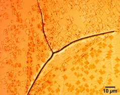 |
| Optical micrograph showing graphene domains formed across grain boundaries. |
Abstract:
A new way of growing graphene without the defects that weaken it and prevent electrons from flowing freely within it could open the way to large-scale manufacturing of graphene-based devices with applications in fields such as electronics, energy, and healthcare.
Routes towards defect-free graphene
Oxford, UK | Posted on February 1st, 2013A team led by Oxford University scientists has overcome a key problem of growing graphene - a one atom-thick layer of carbon - when using an established technique called chemical vapour deposition, that the tiny flakes of graphene form with random orientations, leaving defects or 'seams' between flakes that grow together.
The discovery, reported in a paper to be published in ACS Nano, reveals how these graphene flakes, known as 'domains', can be lined up by manipulating the alignment of carbon atoms on a relatively cheap copper foil - the atomic structure of the copper surface acts as a 'guide' that controls the orientation of the carbon atoms growing on top of them.
A combination of control of this copper guide and the pressure applied during growth makes it possible to control the thickness of these domains, the geometry of their edges and the grain boundaries where they meet - 'seams' that act as obstacles to the smooth progress of electrons necessary to create efficient graphene-based electrical and electronic devices.
'Current methods of growing flakes of graphene often suffer from graphene domains not lining up,' said Professor Nicole Grobert of Oxford University's Department of Materials who led the work. 'Our discovery shows that it is possible to produce large sheets of graphene where these flakes, called 'domains', are well-aligned, which will create a neater, stronger, and more 'electron-friendly' material.'
In principle the size of the sheet of graphene that can be created is only limited by the size of the copper base sheet.
The Oxford-led team, which includes researchers from Forschungszentrum Juelich Germany, the University of Ioannina Greece, and Renishaw plc, has shown that it is also possible using the new technique to selectively grow bilayer domains of graphene - a double layer of closely packed carbon atoms - which are of particular interest for their unusual electrical properties.
'People have used copper as a base material before, but this is the first time anyone has shown that the many different types of copper surfaces can indeed strongly control the structure of graphene,' said Professor Grobert. 'It's an important step towards finding a way of manufacturing graphene in a controlled fashion at an industrial scale, something that is essential if we are to bridge the gap between fundamental research and building useful graphene-based technologies.'
####
For more information, please click here
Contacts:
University of Oxford Press Office
44-018-652-83877
Copyright © University of Oxford
If you have a comment, please Contact us.Issuers of news releases, not 7th Wave, Inc. or Nanotechnology Now, are solely responsible for the accuracy of the content.
Bookmark:


| Related News Press |
News and information
![]() Decoding hydrogen‑bond network of electrolyte for cryogenic durable aqueous zinc‑ion batteries January 30th, 2026
Decoding hydrogen‑bond network of electrolyte for cryogenic durable aqueous zinc‑ion batteries January 30th, 2026
![]() COF scaffold membrane with gate‑lane nanostructure for efficient Li+/Mg2+ separation January 30th, 2026
COF scaffold membrane with gate‑lane nanostructure for efficient Li+/Mg2+ separation January 30th, 2026
Graphene/ Graphite
![]() Electrifying results shed light on graphene foam as a potential material for lab grown cartilage June 6th, 2025
Electrifying results shed light on graphene foam as a potential material for lab grown cartilage June 6th, 2025
![]() Breakthrough in proton barrier films using pore-free graphene oxide: Kumamoto University researchers achieve new milestone in advanced coating technologies September 13th, 2024
Breakthrough in proton barrier films using pore-free graphene oxide: Kumamoto University researchers achieve new milestone in advanced coating technologies September 13th, 2024
Possible Futures
![]() Decoding hydrogen‑bond network of electrolyte for cryogenic durable aqueous zinc‑ion batteries January 30th, 2026
Decoding hydrogen‑bond network of electrolyte for cryogenic durable aqueous zinc‑ion batteries January 30th, 2026
![]() COF scaffold membrane with gate‑lane nanostructure for efficient Li+/Mg2+ separation January 30th, 2026
COF scaffold membrane with gate‑lane nanostructure for efficient Li+/Mg2+ separation January 30th, 2026
Chip Technology
![]() Metasurfaces smooth light to boost magnetic sensing precision January 30th, 2026
Metasurfaces smooth light to boost magnetic sensing precision January 30th, 2026
![]() Beyond silicon: Electronics at the scale of a single molecule January 30th, 2026
Beyond silicon: Electronics at the scale of a single molecule January 30th, 2026
![]() Lab to industry: InSe wafer-scale breakthrough for future electronics August 8th, 2025
Lab to industry: InSe wafer-scale breakthrough for future electronics August 8th, 2025
Nanomedicine
![]() New molecular technology targets tumors and simultaneously silences two �undruggable� cancer genes August 8th, 2025
New molecular technology targets tumors and simultaneously silences two �undruggable� cancer genes August 8th, 2025
![]() New imaging approach transforms study of bacterial biofilms August 8th, 2025
New imaging approach transforms study of bacterial biofilms August 8th, 2025
![]() Cambridge chemists discover simple way to build bigger molecules � one carbon at a time June 6th, 2025
Cambridge chemists discover simple way to build bigger molecules � one carbon at a time June 6th, 2025
![]() Electrifying results shed light on graphene foam as a potential material for lab grown cartilage June 6th, 2025
Electrifying results shed light on graphene foam as a potential material for lab grown cartilage June 6th, 2025
Discoveries
![]() From sensors to smart systems: the rise of AI-driven photonic noses January 30th, 2026
From sensors to smart systems: the rise of AI-driven photonic noses January 30th, 2026
![]() Decoding hydrogen‑bond network of electrolyte for cryogenic durable aqueous zinc‑ion batteries January 30th, 2026
Decoding hydrogen‑bond network of electrolyte for cryogenic durable aqueous zinc‑ion batteries January 30th, 2026
![]() COF scaffold membrane with gate‑lane nanostructure for efficient Li+/Mg2+ separation January 30th, 2026
COF scaffold membrane with gate‑lane nanostructure for efficient Li+/Mg2+ separation January 30th, 2026
Announcements
![]() Decoding hydrogen‑bond network of electrolyte for cryogenic durable aqueous zinc‑ion batteries January 30th, 2026
Decoding hydrogen‑bond network of electrolyte for cryogenic durable aqueous zinc‑ion batteries January 30th, 2026
![]() COF scaffold membrane with gate‑lane nanostructure for efficient Li+/Mg2+ separation January 30th, 2026
COF scaffold membrane with gate‑lane nanostructure for efficient Li+/Mg2+ separation January 30th, 2026
Energy
![]() Sensors innovations for smart lithium-based batteries: advancements, opportunities, and potential challenges August 8th, 2025
Sensors innovations for smart lithium-based batteries: advancements, opportunities, and potential challenges August 8th, 2025
![]() Simple algorithm paired with standard imaging tool could predict failure in lithium metal batteries August 8th, 2025
Simple algorithm paired with standard imaging tool could predict failure in lithium metal batteries August 8th, 2025
Industrial
![]() Tiny nanosheets, big leap: A new sensor detects ethanol at ultra-low levels January 30th, 2026
Tiny nanosheets, big leap: A new sensor detects ethanol at ultra-low levels January 30th, 2026
![]() Quantum interference in molecule-surface collisions February 28th, 2025
Quantum interference in molecule-surface collisions February 28th, 2025
![]() Boron nitride nanotube fibers get real: Rice lab creates first heat-tolerant, stable fibers from wet-spinning process June 24th, 2022
Boron nitride nanotube fibers get real: Rice lab creates first heat-tolerant, stable fibers from wet-spinning process June 24th, 2022
|
|
||
|
|
||
| The latest news from around the world, FREE | ||
|
|
||
|
|
||
| Premium Products | ||
|
|
||
|
Only the news you want to read!
Learn More |
||
|
|
||
|
Full-service, expert consulting
Learn More |
||
|
|
||