Home > Press > Penn Researchers Show New Level of Control Over Liquid Crystals
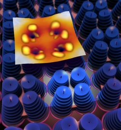 |
| Manipulating the surface of liquid crystals. (Art courtesy of Felice Macera, Daniel Beller, Apiradee Honglawan and Simon Čopar) |
Abstract:
Directed assembly is a growing field of research in nanotechnology in which scientists and engineers aim to manufacture structures on the smallest scales without having to individually manipulate each component. Rather, they set out precisely defined starting conditions and let the physics and chemistry that govern those components do the rest.
Penn Researchers Show New Level of Control Over Liquid Crystals
Philadelphia, PA | Posted on January 7th, 2013An interdisciplinary team of researchers from the University of Pennsylvania has shown a new way to direct the assembly of liquid crystals, generating small features that spontaneously arrange in arrays based on much larger templates.
The study was led by Shu Yang, associate professor in the School of Engineering and Applied Science's departments of Materials Science and Engineering and Chemical and Biomolecular Engineering; Kathleen Stebe, Engineering's vice dean for research and professor in Chemical and Biomolecular Engineering; and Randall Kamien, professor in the School of Arts and Sciences' Department of Physics and Astronomy. Apiradee Honglawan of Yang's lab, Daniel Beller of Kamien's group and Marcello Cavallaro Jr. of Stebe's lab also contributed to the research.
They came together through Penn's Materials Research Science and Engineering Center, which recently received a $21.7 million National Science Foundation grant to support this kind of interdisciplinary research. Stebe and Kamien are leaders of the Center's sub-group focused on elasticity in soft materials and knew they had the expertise on hand to do groundbreaking work with liquid crystals.
Their work was published in the Proceedings of the National Academies of Science.
Crystals are materials that have molecules arrayed in regular three-dimensional patterns; liquid crystals contain some, but not all, of these patterns, and their molecules can flow around one another and change the direction they face. This behavior allows defects, places on the surface where the molecular orientation of the liquid crystals is disrupted.
Despite their name, such defects are highly desirable. If the location of the defects can be controlled, the change in pattern or orientation can be put to use. In a liquid crystal display, for example, the crystals' orientation in different regions determines which parts of the screen are illuminated.
"Liquid crystals naturally produce a pattern of close-packed defects on their surfaces," Yang said, "but it turns out that this pattern is often not that interesting for device applications. We want to arbitrarily manipulate that pattern on demand."
Electrical fields are often used to change the crystals' orientation, as in the case with liquid crystal displays, but the Penn research team was interested in manipulating defects by using a physical template. Employing a class of liquid crystals that forms stacks of layers spaced in nanometers � known as "smectic" liquid crystals � the researchers set out to show that, by altering the geometry of the molecules on the bottommost layer, they could produce changes in the patterns of defects on the topmost.
"The molecules can feel the geometry of the template, which creates a sort of elastic cue," Stebe said. "That cue is transmitted layer by layer, and the whole system responds."
The researchers' template was a series of microscopic posts arrayed like a bed of nails. By altering the size, shape, symmetry and spacing of these posts, as well as the thickness of the liquid crystal film, the researchers discovered they could make subtle changes in the patterns of the defects.
For example, a smectic liquid crystal that would naturally form a hexagonal array of dimple-like defects on its surface could be templated to form a square pattern or to have dimples that were more closely or loosely packed.
Critically, these induced defect patterns weren't one-to-one reproductions of the pattern of posts on the template layer. The researchers were able to generate more complex relationships, such as getting four defects to sit atop each circular post or defects that formed over the points of a triangular post. They were also able to deduce the rules that govern these relationships and predict what defect patterns a given set of post parameters would produce.
"The first layer's molecules tend to be pinned to the edges of the posts," Kamien said, "so changing a post's size and shape will change how many defects can sit on its edges at the same time."
The size discrepancy between the posts and individual molecules of the liquid crystal is also a key feature for using this class of liquid crystal in directed assembly. The posts are each a few microns wide and tall, still microscopically small, but large enough to be easily and economically made to specification. This is much more attractive than trying to directly control the size and arrangement of the liquid crystals' defects.
"The liquid crystal layers are very thin, so the defects are on the order of several nanometers across" Kamien said. "Those defects would normally be very hard to control, especially compared to the posts, which are more like a few thousand nanometers across."
Beyond sensors and displays, these defects can be used in nanomanufacturing.
"If you make defects like dimples, you could put ink in them and use them like a stamp," Kamien said. "Or you could make the inverse of the dimples and make points, which could be used as localized surface plasmon resonance hot spots for chemical and biological sensing or as a topographic protrusion for creating a superhydrophobic surface."
And because the layers of liquid crystals transmit elastic energy, they can also be used to do mechanical work. This means that the top layer could be used as a template to assemble even larger molecules.
"You could put nanoparticles, quantum dots or carbon nanotubes in the liquid crystal layers and they would be expelled into to the defects," Yang said.
A template consisting of circular posts could even be dynamically altered with heat and an electric field, for example, making the posts in a certain region elliptical. This microscopic geometric cue would travel up the layers of liquid crystal and produce micrometer-scale changes on the surface.
By establishing the mathematical relationships between the post parameters and the surface-layer defects, the researchers are laying the foundation of a directed assembly technique that can be used with any smectic liquid crystal.
"We are providing a very crude cue and getting exquisite molecular level organization," Stebe said. "Any liquid crystal that makes layers can now be used to make rather beautiful control over textures on the surface.
The research was supported by the National Science Foundation.
####
For more information, please click here
Contacts:
Evan Lerner
215-573-6604
Copyright © University of Pennsylvania
If you have a comment, please Contact us.Issuers of news releases, not 7th Wave, Inc. or Nanotechnology Now, are solely responsible for the accuracy of the content.
Bookmark:


| Related News Press |
News and information
![]() Quantum computer improves AI predictions April 17th, 2026
Quantum computer improves AI predictions April 17th, 2026
![]() Flexible sensor gains sensitivity under pressure April 17th, 2026
Flexible sensor gains sensitivity under pressure April 17th, 2026
![]() A reusable chip for particulate matter sensing April 17th, 2026
A reusable chip for particulate matter sensing April 17th, 2026
![]() Detecting vibrational quantum beating in the predissociation dynamics of SF6 using time-resolved photoelectron spectroscopy April 17th, 2026
Detecting vibrational quantum beating in the predissociation dynamics of SF6 using time-resolved photoelectron spectroscopy April 17th, 2026
Physics
![]() UC Irvine physicists discover method to reverse �quantum scrambling� : The work addresses the problem of information loss in quantum computing system April 17th, 2026
UC Irvine physicists discover method to reverse �quantum scrambling� : The work addresses the problem of information loss in quantum computing system April 17th, 2026
Chemistry
![]() Projecting light to dispense liquids: A new route to ultra-precise microdroplets January 30th, 2026
Projecting light to dispense liquids: A new route to ultra-precise microdroplets January 30th, 2026
![]() From sensors to smart systems: the rise of AI-driven photonic noses January 30th, 2026
From sensors to smart systems: the rise of AI-driven photonic noses January 30th, 2026
![]() "Nanoreactor" cage uses visible light for catalytic and ultra-selective cross-cycloadditions October 3rd, 2025
"Nanoreactor" cage uses visible light for catalytic and ultra-selective cross-cycloadditions October 3rd, 2025
![]() Cambridge chemists discover simple way to build bigger molecules � one carbon at a time June 6th, 2025
Cambridge chemists discover simple way to build bigger molecules � one carbon at a time June 6th, 2025
Display technology/LEDs/SS Lighting/OLEDs
![]() Spinel-type sulfide semiconductors to operate the next-generation LEDs and solar cells For solar-cell absorbers and green-LED source October 3rd, 2025
Spinel-type sulfide semiconductors to operate the next-generation LEDs and solar cells For solar-cell absorbers and green-LED source October 3rd, 2025
Govt.-Legislation/Regulation/Funding/Policy
![]() Quantum computer improves AI predictions April 17th, 2026
Quantum computer improves AI predictions April 17th, 2026
![]() Metasurfaces smooth light to boost magnetic sensing precision January 30th, 2026
Metasurfaces smooth light to boost magnetic sensing precision January 30th, 2026
![]() New imaging approach transforms study of bacterial biofilms August 8th, 2025
New imaging approach transforms study of bacterial biofilms August 8th, 2025
Self Assembly
![]() Diamond glitter: A play of colors with artificial DNA crystals May 17th, 2024
Diamond glitter: A play of colors with artificial DNA crystals May 17th, 2024
![]() Liquid crystal templated chiral nanomaterials October 14th, 2022
Liquid crystal templated chiral nanomaterials October 14th, 2022
![]() Nanoclusters self-organize into centimeter-scale hierarchical assemblies April 22nd, 2022
Nanoclusters self-organize into centimeter-scale hierarchical assemblies April 22nd, 2022
![]() Atom by atom: building precise smaller nanoparticles with templates March 4th, 2022
Atom by atom: building precise smaller nanoparticles with templates March 4th, 2022
Nanotubes/Buckyballs/Fullerenes/Nanorods/Nanostrings/Nanosheets
![]() Tiny nanosheets, big leap: A new sensor detects ethanol at ultra-low levels January 30th, 2026
Tiny nanosheets, big leap: A new sensor detects ethanol at ultra-low levels January 30th, 2026
![]() Enhancing power factor of p- and n-type single-walled carbon nanotubes April 25th, 2025
Enhancing power factor of p- and n-type single-walled carbon nanotubes April 25th, 2025
![]() Chainmail-like material could be the future of armor: First 2D mechanically interlocked polymer exhibits exceptional flexibility and strength January 17th, 2025
Chainmail-like material could be the future of armor: First 2D mechanically interlocked polymer exhibits exceptional flexibility and strength January 17th, 2025
![]() Innovative biomimetic superhydrophobic coating combines repair and buffering properties for superior anti-erosion December 13th, 2024
Innovative biomimetic superhydrophobic coating combines repair and buffering properties for superior anti-erosion December 13th, 2024
Discoveries
![]() Quantum computer improves AI predictions April 17th, 2026
Quantum computer improves AI predictions April 17th, 2026
![]() Flexible sensor gains sensitivity under pressure April 17th, 2026
Flexible sensor gains sensitivity under pressure April 17th, 2026
![]() A reusable chip for particulate matter sensing April 17th, 2026
A reusable chip for particulate matter sensing April 17th, 2026
![]() Detecting vibrational quantum beating in the predissociation dynamics of SF6 using time-resolved photoelectron spectroscopy April 17th, 2026
Detecting vibrational quantum beating in the predissociation dynamics of SF6 using time-resolved photoelectron spectroscopy April 17th, 2026
Announcements
![]() A fundamentally new therapeutic approach to cystic fibrosis: Nanobody repairs cellular defect April 17th, 2026
A fundamentally new therapeutic approach to cystic fibrosis: Nanobody repairs cellular defect April 17th, 2026
![]() UC Irvine physicists discover method to reverse �quantum scrambling� : The work addresses the problem of information loss in quantum computing system April 17th, 2026
UC Irvine physicists discover method to reverse �quantum scrambling� : The work addresses the problem of information loss in quantum computing system April 17th, 2026
Quantum Dots/Rods
![]() A new kind of magnetism November 17th, 2023
A new kind of magnetism November 17th, 2023
![]() IOP Publishing celebrates World Quantum Day with the announcement of a special quantum collection and the winners of two prestigious quantum awards April 14th, 2023
IOP Publishing celebrates World Quantum Day with the announcement of a special quantum collection and the winners of two prestigious quantum awards April 14th, 2023
![]() Qubits on strong stimulants: Researchers find ways to improve the storage time of quantum information in a spin rich material January 27th, 2023
Qubits on strong stimulants: Researchers find ways to improve the storage time of quantum information in a spin rich material January 27th, 2023
![]() NIST�s grid of quantum islands could reveal secrets for powerful technologies November 18th, 2022
NIST�s grid of quantum islands could reveal secrets for powerful technologies November 18th, 2022
|
|
||
|
|
||
| The latest news from around the world, FREE | ||
|
|
||
|
|
||
| Premium Products | ||
|
|
||
|
Only the news you want to read!
Learn More |
||
|
|
||
|
Full-service, expert consulting
Learn More |
||
|
|
||