Home > Press > Imec presents an ultra-thin hybrid floating gate cell at IEDM2012: The results are an important enabler for further scaling of NAND Flash technology
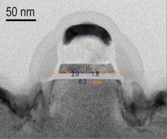 |
| TEM of Ultra thin Hybrid Floating Gate (HFG) with high-k Inter Gate Dielectric (IGD) extending Flash scaling beyond 1x node |
Abstract:
Imec announces that it has developed an ultra-thin hybrid floating gate cell with demonstrated functionality. The results, which are presented at this week's 2012 IEEE International Electron Devices Meeting (IEDM, San Francisco, USA, December 10-12, 2012), are an important step for further scaling of NAND Flash technology towards the 10nm half pitch node and beyond.
The increasing need for high density flash memory has driven the scaling of the technology down to the 19nm half pitch node which is currently in production. However, from such dimensions on, the Control Gate (CG) can no longer be wrapped around the Floating Gate (FG), urging for a planar floating gate architecture. But planarising the technology results in a reduced coupling of the CG and FG. Consequently, the performance degrades due to leakage through the Interpoly dielectric (IPD). In order to recover the performance in planar devices, imec has developed a Hybrid Floating Gate (HFG) architecture featuring a low work function material at the bottom and a high work function material at the top. The functionality has been successfully demonstrated in integrated cells. Moreover, to limit the cell to cell interference occurring in a high-density NAND array, imec scaled down the thickness of the hybrid floating gate to only 4nm.
Imec presents an ultra-thin hybrid floating gate cell at IEDM2012: The results are an important enabler for further scaling of NAND Flash technology
San Francisco, CA | Posted on December 12th, 2012Jan Van Houdt, Director of the Flash memory program at imec: "Flash memory is the state-of-the-art technology in all mobile devices, ranging from cell phones, digital cameras, USB sticks, MP3 players and tablets, to solid state drives. To address the exploding demand for memory capacity in such devices, imec is pushing the roadmap of the current Flash technology. We are excited to have demonstrated this functional ultra-thin hybrid floating gate cell technology, as an enabling solution for our partners to scale Flash memory down to 10nm and further increase the memory capacity in next-generation mobile devices".
These results were obtained in cooperation with imec's key memory partners INTEL, Micron, Samsung, SanDisk, Toshiba and SK Hynix.
####
About IMEC
Imec performs world-leading research in nanoelectronics. Imec leverages its scientific knowledge with the innovative power of its global partnerships in ICT, healthcare and energy. Imec delivers industry-relevant technology solutions. In a unique high-tech environment, its international top talent is committed to providing the building blocks for a better life in a sustainable society. Imec is headquartered in Leuven, Belgium, and has offices in Belgium, the Netherlands, Taiwan, US, China, India and Japan. Its staff of close to 2,000 people includes more than 600 industrial residents and guest researchers. In 2011, imec's revenue (P&L) was about 300 million euro. Further information on imec can be found at www.imec.be.
Imec is a registered trademark for the activities of IMEC International (a legal entity set up under Belgian law as a "stichting van openbaar nut�), imec Belgium (IMEC vzw supported by the Flemish Government), imec the Netherlands (Stichting IMEC Nederland, part of Holst Centre which is supported by the Dutch Government), imec Taiwan (IMEC Taiwan Co.) and imec China (IMEC Microelectronics (Shangai) Co. Ltd.) and imec India (Imec India Private Limited).
For more information, please click here
Contacts:
Hanne Degans
External communications officer
T: +32 16 28 17 69
Mobile : +32 486 06 51 75
Olga Walsh
Business Technology
[ f o r m u l a ]
Formula PR, Inc.
1215 Cushman Avenue
San Diego, CA 92110
Office 619-234-0345
Copyright © IMEC
If you have a comment, please Contact us.Issuers of news releases, not 7th Wave, Inc. or Nanotechnology Now, are solely responsible for the accuracy of the content.
Bookmark:


| Related News Press |
News and information
![]() Simulating magnetization in a Heisenberg quantum spin chain April 5th, 2024
Simulating magnetization in a Heisenberg quantum spin chain April 5th, 2024
![]() NRL charters Navy�s quantum inertial navigation path to reduce drift April 5th, 2024
NRL charters Navy�s quantum inertial navigation path to reduce drift April 5th, 2024
![]() Discovery points path to flash-like memory for storing qubits: Rice find could hasten development of nonvolatile quantum memory April 5th, 2024
Discovery points path to flash-like memory for storing qubits: Rice find could hasten development of nonvolatile quantum memory April 5th, 2024
Chip Technology
![]() Discovery points path to flash-like memory for storing qubits: Rice find could hasten development of nonvolatile quantum memory April 5th, 2024
Discovery points path to flash-like memory for storing qubits: Rice find could hasten development of nonvolatile quantum memory April 5th, 2024
![]() Utilizing palladium for addressing contact issues of buried oxide thin film transistors April 5th, 2024
Utilizing palladium for addressing contact issues of buried oxide thin film transistors April 5th, 2024
![]() HKUST researchers develop new integration technique for efficient coupling of III-V and silicon February 16th, 2024
HKUST researchers develop new integration technique for efficient coupling of III-V and silicon February 16th, 2024
Memory Technology
![]() Utilizing palladium for addressing contact issues of buried oxide thin film transistors April 5th, 2024
Utilizing palladium for addressing contact issues of buried oxide thin film transistors April 5th, 2024
![]() Interdisciplinary: Rice team tackles the future of semiconductors Multiferroics could be the key to ultralow-energy computing October 6th, 2023
Interdisciplinary: Rice team tackles the future of semiconductors Multiferroics could be the key to ultralow-energy computing October 6th, 2023
![]() Researchers discover materials exhibiting huge magnetoresistance June 9th, 2023
Researchers discover materials exhibiting huge magnetoresistance June 9th, 2023
Announcements
![]() NRL charters Navy�s quantum inertial navigation path to reduce drift April 5th, 2024
NRL charters Navy�s quantum inertial navigation path to reduce drift April 5th, 2024
![]() Discovery points path to flash-like memory for storing qubits: Rice find could hasten development of nonvolatile quantum memory April 5th, 2024
Discovery points path to flash-like memory for storing qubits: Rice find could hasten development of nonvolatile quantum memory April 5th, 2024
Events/Classes
![]() Researchers demonstrate co-propagation of quantum and classical signals: Study shows that quantum encryption can be implemented in existing fiber networks January 20th, 2023
Researchers demonstrate co-propagation of quantum and classical signals: Study shows that quantum encryption can be implemented in existing fiber networks January 20th, 2023
Research partnerships
![]() Discovery points path to flash-like memory for storing qubits: Rice find could hasten development of nonvolatile quantum memory April 5th, 2024
Discovery points path to flash-like memory for storing qubits: Rice find could hasten development of nonvolatile quantum memory April 5th, 2024
![]() Researchers� approach may protect quantum computers from attacks March 8th, 2024
Researchers� approach may protect quantum computers from attacks March 8th, 2024
![]() 'Sudden death' of quantum fluctuations defies current theories of superconductivity: Study challenges the conventional wisdom of superconducting quantum transitions January 12th, 2024
'Sudden death' of quantum fluctuations defies current theories of superconductivity: Study challenges the conventional wisdom of superconducting quantum transitions January 12th, 2024
|
|
||
|
|
||
| The latest news from around the world, FREE | ||
|
|
||
|
|
||
| Premium Products | ||
|
|
||
|
Only the news you want to read!
Learn More |
||
|
|
||
|
Full-service, expert consulting
Learn More |
||
|
|
||