Home > Press > Research discovery could revolutionise semiconductor manufacture
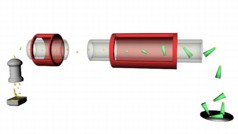 |
| Aerotaxy production process |
Abstract:
A completely new method of manufacturing the smallest structures in electronics could make their manufacture thousands of times quicker, allowing for cheaper semiconductors. The findings have been published in the latest issue of Nature.
Research discovery could revolutionise semiconductor manufacture
Germany | Posted on December 1st, 2012Instead of starting from a silicon wafer or other substrate, as is usual today, researchers have made it possible for the structures to grow from freely suspended nanoparticles of gold in a flowing gas.
Behind the discovery is Lars Samuelson, Professor of Semiconductor Physics at Lund University, Sweden, and head of the University's Nanometre Structure Consortium. He believes the technology will be ready for commercialisation in two to four years' time. A prototype for solar cells is expected to be completed in two years.
"When I first suggested the idea of getting rid of the substrate, people around me said �you're out of your mind, Lars; that would never work'. When we tested the principle in one of our converted ovens at 400�C, the results were better than we could have dreamt of", he says.
"The basic idea was to let nanoparticles of gold serve as a substrate from which the semiconductors grow. This means that the accepted concepts really were turned upside down!"
Since then, the technology has been refined, patents have been obtained and further studies have been conducted. In the article in Nature, the researchers show how the growth can be controlled using temperature, time and the size of the gold nanoparticles.
Recently, they have also built a prototype machine with a specially built oven. Using a series of ovens, the researchers expect to be able to �bake' the nanowires, as the structures are called, and thereby develop multiple variants, such as p-n diodes. A further advantage of the technology is avoiding the cost of expensive semiconductor wafers.
"In addition, the process is not only extremely quick, it is also continuous. Traditional manufacture of substrates is batch-based and is therefore much more time-consuming", adds Lars Samuelson.
At the moment, the researchers are working to develop a good method to capture the nanowires and make them self-assemble in an ordered manner on a specific surface. This could be glass, steel or another material suited to the purpose. The reason why no one has tested this method before, in the view of Professor Samuelson, is that today's method is so basic and obvious. Such things tend to be difficult to question.
However, the Lund researchers have a head start thanks to their parallel research based on an innovative method in the manufacture of nanowires on semiconductor wafers, known as epitaxy - consequently, the researchers have chosen to call the new method aerotaxy. Instead of sculpting structures out of silicon or another semiconductor material, the structures are instead allowed to develop, atomic layer by atomic layer, through controlled self-organisation.
The structures are referred to as nanowires or nanorods. The breakthrough for these semiconductor structures came in 2002 and research on them is primarily carried out at Lund, Berkeley and Harvard universities.
The Lund researchers specialise in developing the physical and electrical properties of the wires, which helps create better and more energy-saving solar cells, LEDs, batteries and other electrical equipment that is now an integrated part of our lives.
####
For more information, please click here
Copyright © Wiley-VCH Materials Science Journals
If you have a comment, please Contact us.Issuers of news releases, not 7th Wave, Inc. or Nanotechnology Now, are solely responsible for the accuracy of the content.
Bookmark:


| Related Links |
| Related News Press |
News and information
![]() Simulating magnetization in a Heisenberg quantum spin chain April 5th, 2024
Simulating magnetization in a Heisenberg quantum spin chain April 5th, 2024
![]() NRL charters Navy�s quantum inertial navigation path to reduce drift April 5th, 2024
NRL charters Navy�s quantum inertial navigation path to reduce drift April 5th, 2024
![]() Discovery points path to flash-like memory for storing qubits: Rice find could hasten development of nonvolatile quantum memory April 5th, 2024
Discovery points path to flash-like memory for storing qubits: Rice find could hasten development of nonvolatile quantum memory April 5th, 2024
Chip Technology
![]() Discovery points path to flash-like memory for storing qubits: Rice find could hasten development of nonvolatile quantum memory April 5th, 2024
Discovery points path to flash-like memory for storing qubits: Rice find could hasten development of nonvolatile quantum memory April 5th, 2024
![]() Utilizing palladium for addressing contact issues of buried oxide thin film transistors April 5th, 2024
Utilizing palladium for addressing contact issues of buried oxide thin film transistors April 5th, 2024
![]() HKUST researchers develop new integration technique for efficient coupling of III-V and silicon February 16th, 2024
HKUST researchers develop new integration technique for efficient coupling of III-V and silicon February 16th, 2024
Discoveries
![]() Chemical reactions can scramble quantum information as well as black holes April 5th, 2024
Chemical reactions can scramble quantum information as well as black holes April 5th, 2024
![]() New micromaterial releases nanoparticles that selectively destroy cancer cells April 5th, 2024
New micromaterial releases nanoparticles that selectively destroy cancer cells April 5th, 2024
![]() Utilizing palladium for addressing contact issues of buried oxide thin film transistors April 5th, 2024
Utilizing palladium for addressing contact issues of buried oxide thin film transistors April 5th, 2024
Announcements
![]() NRL charters Navy�s quantum inertial navigation path to reduce drift April 5th, 2024
NRL charters Navy�s quantum inertial navigation path to reduce drift April 5th, 2024
![]() Discovery points path to flash-like memory for storing qubits: Rice find could hasten development of nonvolatile quantum memory April 5th, 2024
Discovery points path to flash-like memory for storing qubits: Rice find could hasten development of nonvolatile quantum memory April 5th, 2024
|
|
||
|
|
||
| The latest news from around the world, FREE | ||
|
|
||
|
|
||
| Premium Products | ||
|
|
||
|
Only the news you want to read!
Learn More |
||
|
|
||
|
Full-service, expert consulting
Learn More |
||
|
|
||