Home > Press > USC scientists 'clone' carbon nanotubes to unlock their potential for use in electronics: Using a new method, researchers can now grow carbon nanotube semiconductors of predefined structures, which may pave the way for carbon to be used in future electronics
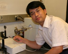 |
| Chongwu Zhou holds up a piece of plastic substrate used to build nanoscale transistors and circuits. |
Abstract:
The heart of the computer industry is known as "Silicon Valley" for a reason. Integrated circuit computer chips have been made from silicon since computing's infancy in the 1960s. Now, thanks to a team of USC researchers, carbon nanotubes may emerge as a contender to silicon's throne.
USC scientists 'clone' carbon nanotubes to unlock their potential for use in electronics: Using a new method, researchers can now grow carbon nanotube semiconductors of predefined structures, which may pave the way for carbon to be used in future electronics
Los Angeles, CA | Posted on November 14th, 2012Scientists and industry experts have long speculated that carbon nanotube transistors would one day replace their silicon predecessors. In 1998, Delft University built the world's first carbon nanotube transistors - carbon nanotubes have the potential to be far smaller, faster, and consume less power than silicon transistors.
A key reason carbon nanotubes are not in your computer right now is that they are difficult to manufacture in a predictable way. Scientists have had a difficult time controlling the manufacture of nanotubes to the correct diameter, type and ultimately chirality, factors that control nanotubes' electrical and mechanical properties.
Think of chirality like this: if you took a sheet of notebook paper and rolled it straight up into a tube, it would have a certain chirality. If you rolled that same sheet up at an angle, it would have a different chirality. In this example, the notebook paper represents a sheet of latticed carbon atoms that are rolled-up to create a nanotube.
A team led by Professor Chongwu Zhou of the USC Viterbi School of Engineering and Ming Zheng of the National Institute of Standards and Technology in Maryland solved the problem by inventing a system that consistently produces carbon nanotubes of a predictable diameter and chirality.
Zhou worked with his group members Jia Liu, Chuan Wang, Bilu Liu, Liang Chen, and Ming Zheng and Xiaomin Tu of the National Institute of Standards and Technology in Maryland.
"Controlling the chirality of carbon nanotubes has been a dream for many researchers. Now the dream has come true." said Zhou. The team has already patented its innovation, and its research will be published Nov. 13 in Nature Communications.
Carbon nanotubes are typically grown using a chemical vapor deposition (CVD) system in which a chemical-laced gas is pumped into a chamber containing substrates with metal catalyst nanoparticles, upon which the nanotubes grow. It is generally believed that the diameters of the nanotubes are determined by the size of the catalytic metal nanoparticles. However, attempts to control the catalysts in hopes of achieving chirality-controlled nanotube growth have not been successful.
The USC team's innovation was to jettison the catalyst and instead plant pieces of carbon nanotubes that have been separated and pre-selected based on chirality, using a nanotube separation technique developed and perfected by Zheng and his coworkers at NIST. Using those pieces as seeds, the team used chemical vapor deposition to extend the seeds to get much longer nanotubes, which were shown to have the same chirality as the seeds..
The process is referred to as "nanotube cloning." The next steps in the research will be to carefully study the mechanism of the nanotube growth in this system, to scale up the cloning process to get large quantities of chirality-controlled nanotubes, and to use those nanotubes for electronic applications
Funding of the USC team for this research came from the Semiconductor Research Corporation's Focus Research Program Functional Engineered Nano Architectonics center and the Office of Naval Research.
####
For more information, please click here
Contacts:
Robert Perkins
213-740-9226
Copyright © University of Southern California
If you have a comment, please Contact us.Issuers of news releases, not 7th Wave, Inc. or Nanotechnology Now, are solely responsible for the accuracy of the content.
Bookmark:


| Related News Press |
News and information
![]() Quantum computer improves AI predictions April 17th, 2026
Quantum computer improves AI predictions April 17th, 2026
![]() Flexible sensor gains sensitivity under pressure April 17th, 2026
Flexible sensor gains sensitivity under pressure April 17th, 2026
![]() A reusable chip for particulate matter sensing April 17th, 2026
A reusable chip for particulate matter sensing April 17th, 2026
![]() Detecting vibrational quantum beating in the predissociation dynamics of SF6 using time-resolved photoelectron spectroscopy April 17th, 2026
Detecting vibrational quantum beating in the predissociation dynamics of SF6 using time-resolved photoelectron spectroscopy April 17th, 2026
Govt.-Legislation/Regulation/Funding/Policy
![]() Quantum computer improves AI predictions April 17th, 2026
Quantum computer improves AI predictions April 17th, 2026
![]() Metasurfaces smooth light to boost magnetic sensing precision January 30th, 2026
Metasurfaces smooth light to boost magnetic sensing precision January 30th, 2026
![]() New imaging approach transforms study of bacterial biofilms August 8th, 2025
New imaging approach transforms study of bacterial biofilms August 8th, 2025
Chip Technology
![]() A reusable chip for particulate matter sensing April 17th, 2026
A reusable chip for particulate matter sensing April 17th, 2026
![]() Metasurfaces smooth light to boost magnetic sensing precision January 30th, 2026
Metasurfaces smooth light to boost magnetic sensing precision January 30th, 2026
Nanotubes/Buckyballs/Fullerenes/Nanorods/Nanostrings/Nanosheets
![]() Tiny nanosheets, big leap: A new sensor detects ethanol at ultra-low levels January 30th, 2026
Tiny nanosheets, big leap: A new sensor detects ethanol at ultra-low levels January 30th, 2026
![]() Enhancing power factor of p- and n-type single-walled carbon nanotubes April 25th, 2025
Enhancing power factor of p- and n-type single-walled carbon nanotubes April 25th, 2025
![]() Chainmail-like material could be the future of armor: First 2D mechanically interlocked polymer exhibits exceptional flexibility and strength January 17th, 2025
Chainmail-like material could be the future of armor: First 2D mechanically interlocked polymer exhibits exceptional flexibility and strength January 17th, 2025
![]() Innovative biomimetic superhydrophobic coating combines repair and buffering properties for superior anti-erosion December 13th, 2024
Innovative biomimetic superhydrophobic coating combines repair and buffering properties for superior anti-erosion December 13th, 2024
Discoveries
![]() Quantum computer improves AI predictions April 17th, 2026
Quantum computer improves AI predictions April 17th, 2026
![]() Flexible sensor gains sensitivity under pressure April 17th, 2026
Flexible sensor gains sensitivity under pressure April 17th, 2026
![]() A reusable chip for particulate matter sensing April 17th, 2026
A reusable chip for particulate matter sensing April 17th, 2026
![]() Detecting vibrational quantum beating in the predissociation dynamics of SF6 using time-resolved photoelectron spectroscopy April 17th, 2026
Detecting vibrational quantum beating in the predissociation dynamics of SF6 using time-resolved photoelectron spectroscopy April 17th, 2026
Announcements
![]() A fundamentally new therapeutic approach to cystic fibrosis: Nanobody repairs cellular defect April 17th, 2026
A fundamentally new therapeutic approach to cystic fibrosis: Nanobody repairs cellular defect April 17th, 2026
![]() UC Irvine physicists discover method to reverse �quantum scrambling� : The work addresses the problem of information loss in quantum computing system April 17th, 2026
UC Irvine physicists discover method to reverse �quantum scrambling� : The work addresses the problem of information loss in quantum computing system April 17th, 2026
Tools
![]() Metasurfaces smooth light to boost magnetic sensing precision January 30th, 2026
Metasurfaces smooth light to boost magnetic sensing precision January 30th, 2026
![]() From sensors to smart systems: the rise of AI-driven photonic noses January 30th, 2026
From sensors to smart systems: the rise of AI-driven photonic noses January 30th, 2026
![]() Japan launches fully domestically produced quantum computer: Expo visitors to experience quantum computing firsthand August 8th, 2025
Japan launches fully domestically produced quantum computer: Expo visitors to experience quantum computing firsthand August 8th, 2025
Military
![]() Quantum engineers �squeeze� laser frequency combs to make more sensitive gas sensors January 17th, 2025
Quantum engineers �squeeze� laser frequency combs to make more sensitive gas sensors January 17th, 2025
![]() Chainmail-like material could be the future of armor: First 2D mechanically interlocked polymer exhibits exceptional flexibility and strength January 17th, 2025
Chainmail-like material could be the future of armor: First 2D mechanically interlocked polymer exhibits exceptional flexibility and strength January 17th, 2025
![]() Single atoms show their true color July 5th, 2024
Single atoms show their true color July 5th, 2024
![]() NRL charters Navy�s quantum inertial navigation path to reduce drift April 5th, 2024
NRL charters Navy�s quantum inertial navigation path to reduce drift April 5th, 2024
|
|
||
|
|
||
| The latest news from around the world, FREE | ||
|
|
||
|
|
||
| Premium Products | ||
|
|
||
|
Only the news you want to read!
Learn More |
||
|
|
||
|
Full-service, expert consulting
Learn More |
||
|
|
||