Home > Press > Making Graphene Industry-Ready: Fluorescence Quenching Metrology
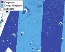 |
| A fluorescence quenching metrology segmented image of graphe fluorinated using a striped mask. |
Abstract:
Researchers at the University of California, Riverside led by Cengiz S. Ozkan have developed a large-scale graphene metrology technique that paves the way for widespread industrial applications, ranging from semiconductors to energy devices.
Making Graphene Industry-Ready: Fluorescence Quenching Metrology
Riverside, CA | Posted on August 16th, 2012Graphene is a carbon allotrope that consists of one-atom-thick planar sheets of carbon atoms. Thanks to its extraordinary electrical, thermal, and optical properties, this miracle carbon material eventually earned its discoverers a Nobel prize in Physics. The greatest challenge in employing graphene industrially, in areas such as energy, semiconductor fabrication, and thermal management, has been making it relevant at larger scales. This requires increasing the size of graphene itself and developing large-scale industrial metrology techniques.
Now the Ozkan group at UCR has made a significant stride in making graphene industry-ready by developing an industrial metrology technique for large-area graphene sheets that relies on fluorescence quenching phenomena. This method is capable of "seeing" chemically functionalized graphene regions and accurately identifying the number of layers in entire large-scale graphene sheets. For utilizing graphene in electronics, an industry-reliable metrology of doped pristine regions, and defect detection are amongst the fundamental needs.
The UCR scientists demonstrate the capability of their method by visualizing complex micron-scale patterns of graphene regions that are chemically modified by fluorine atoms. They went on to test their findings by analyzing the photophysical properties of functionalized and pristine graphene. "Our research demonstrates that fluorescence quenching metrology will provide a widely applicable and scalable characterization technique to visually map complex patterns of chemically altered regions on graphene sheets", said graduate student Maziar Ghazinejad.
Due to its simplicity, small footprint, and high speed, fluorescence quenching metrology is now poised to address the chronic need for an industrial graphene metrology capable of visualizing the features that are being manufactured.
####
For more information, please click here
Copyright © Wiley-VCH Materials Science Journals
If you have a comment, please Contact us.Issuers of news releases, not 7th Wave, Inc. or Nanotechnology Now, are solely responsible for the accuracy of the content.
Bookmark:


| Related Links |
![]() Link to the original paper on Wiley Online Library:
Link to the original paper on Wiley Online Library:
| Related News Press |
News and information
![]() Quantum computer improves AI predictions April 17th, 2026
Quantum computer improves AI predictions April 17th, 2026
![]() Flexible sensor gains sensitivity under pressure April 17th, 2026
Flexible sensor gains sensitivity under pressure April 17th, 2026
![]() A reusable chip for particulate matter sensing April 17th, 2026
A reusable chip for particulate matter sensing April 17th, 2026
![]() Detecting vibrational quantum beating in the predissociation dynamics of SF6 using time-resolved photoelectron spectroscopy April 17th, 2026
Detecting vibrational quantum beating in the predissociation dynamics of SF6 using time-resolved photoelectron spectroscopy April 17th, 2026
Graphene/ Graphite
![]() Electrifying results shed light on graphene foam as a potential material for lab grown cartilage June 6th, 2025
Electrifying results shed light on graphene foam as a potential material for lab grown cartilage June 6th, 2025
![]() Breakthrough in proton barrier films using pore-free graphene oxide: Kumamoto University researchers achieve new milestone in advanced coating technologies September 13th, 2024
Breakthrough in proton barrier films using pore-free graphene oxide: Kumamoto University researchers achieve new milestone in advanced coating technologies September 13th, 2024
Chip Technology
![]() A reusable chip for particulate matter sensing April 17th, 2026
A reusable chip for particulate matter sensing April 17th, 2026
![]() Metasurfaces smooth light to boost magnetic sensing precision January 30th, 2026
Metasurfaces smooth light to boost magnetic sensing precision January 30th, 2026
Discoveries
![]() Quantum computer improves AI predictions April 17th, 2026
Quantum computer improves AI predictions April 17th, 2026
![]() Flexible sensor gains sensitivity under pressure April 17th, 2026
Flexible sensor gains sensitivity under pressure April 17th, 2026
![]() A reusable chip for particulate matter sensing April 17th, 2026
A reusable chip for particulate matter sensing April 17th, 2026
![]() Detecting vibrational quantum beating in the predissociation dynamics of SF6 using time-resolved photoelectron spectroscopy April 17th, 2026
Detecting vibrational quantum beating in the predissociation dynamics of SF6 using time-resolved photoelectron spectroscopy April 17th, 2026
Announcements
![]() A fundamentally new therapeutic approach to cystic fibrosis: Nanobody repairs cellular defect April 17th, 2026
A fundamentally new therapeutic approach to cystic fibrosis: Nanobody repairs cellular defect April 17th, 2026
![]() UC Irvine physicists discover method to reverse �quantum scrambling� : The work addresses the problem of information loss in quantum computing system April 17th, 2026
UC Irvine physicists discover method to reverse �quantum scrambling� : The work addresses the problem of information loss in quantum computing system April 17th, 2026
Tools
![]() Metasurfaces smooth light to boost magnetic sensing precision January 30th, 2026
Metasurfaces smooth light to boost magnetic sensing precision January 30th, 2026
![]() From sensors to smart systems: the rise of AI-driven photonic noses January 30th, 2026
From sensors to smart systems: the rise of AI-driven photonic noses January 30th, 2026
![]() Japan launches fully domestically produced quantum computer: Expo visitors to experience quantum computing firsthand August 8th, 2025
Japan launches fully domestically produced quantum computer: Expo visitors to experience quantum computing firsthand August 8th, 2025
Energy
![]() Sensors innovations for smart lithium-based batteries: advancements, opportunities, and potential challenges August 8th, 2025
Sensors innovations for smart lithium-based batteries: advancements, opportunities, and potential challenges August 8th, 2025
![]() Simple algorithm paired with standard imaging tool could predict failure in lithium metal batteries August 8th, 2025
Simple algorithm paired with standard imaging tool could predict failure in lithium metal batteries August 8th, 2025
|
|
||
|
|
||
| The latest news from around the world, FREE | ||
|
|
||
|
|
||
| Premium Products | ||
|
|
||
|
Only the news you want to read!
Learn More |
||
|
|
||
|
Full-service, expert consulting
Learn More |
||
|
|
||