Home > Press > Ferroelectricity on the Nanoscale: Berkeley Lab Researchers Say First Atomic-Scale Look at Ferroelectric Nanocrystals Points to Terabytes/Inch Storage
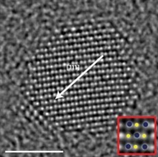 |
| Atomic-resolution images of germanium telluride nanoparticles from Berkeley Lab�s TEAM I electron microscope. |
Abstract:
Promising news for those who relish the prospects of a one-inch chip storing multiple terabytes of data, some clarity has been brought to the here-to-fore confusing physics of ferroelectric nanomaterials. A multi-institutional team of researchers, led by scientists at the U.S. Department of Energy (DOE)'s Lawrence Berkeley National Laboratory (Berkeley Lab) has provided the first atomic-scale insights into the ferroelectric properties of nanocrystals. This information will be critical for development of the next generation of nonvolatile data storage devices.
Ferroelectricity on the Nanoscale: Berkeley Lab Researchers Say First Atomic-Scale Look at Ferroelectric Nanocrystals Points to Terabytes/Inch Storage
Berkeley, CA | Posted on July 10th, 2012Working with the world's most powerful transmission electron microscope, the researchers mapped the ferroelectric structural distortions in nanocrystals of germanium telluride, a semiconductor, and barium titanate, an insulator. This data was then combined with data from electron holographic polarization imaging to yield detailed information on the polarization structures and scaling limits of ferroelectric order on the nanoscale.
"As we scale down our device technology from the microscale to the nanoscale, we need a better understanding of how critical material properties, such as ferroelectric behavior, are impacted," says Paul Alivisatos, director of Berkeley Lab and one of the principal investigators in this research. "Our results provide a pathway to unraveling the fundamental physics of nanoscale ferroelectricity at the smallest possible size scales."
Alivisatos, who is also the Larry and Diane Bock Professor of Nanotechnology at the University of California (UC) Berkeley, is a corresponding author of a paper describing this work in the journal Nature Materials titled "Ferroelectric order in individual nanometrescale Crystals." The other corresponding author is Ramamoorthy Ramesh, a senior scientist with Berkeley Lab's Materials Sciences Division and the Plato Malozemoff Professor of Materials Science and Physics for UC Berkeley.
Ferroelectricity is the property by which materials can be electrically polarized, meaning they will be oriented in favor of either a positive or negative electrical charge. This polarization can be flipped with the application of an external electrical field, a property that could be exploited for nonvolatile data storage, similar to the use of ferromagnetic materials today but using much smaller, far more densely packed devices.
"Although much progress has been made towards understanding nanoscale photophysical magnetic and other functional properties, understanding the basic physics of ferroelectric nanomaterials remains far less advanced," says co-principal investigator Ramesh, who attributes contradicting reports on nanoscale ferroelectricity in part to the lack of high-quality, nanocrystals of ferroelectric materials that feature well-defined sizes, shapes and surfaces.
"Another problem has been the reliance on ensemble measurements rather than single particle techniques," he says. "Statistical-average measurement techniques tend to obscure the physical mechanisms responsible for profound changes in ferroelectric behavior within individual nanocrystals."
The Berkeley Lab-led research team was able to map ferroelectric structural distortions within individual nanocrystals thanks to the unprecedented capabilities of TEAM I, which is housed at Berkeley Lab's National Center for Electron Microscopy (NCEM). TEAM stands for "Transmission Electron Aberration-corrected Microscope." TEAM I can resolve images of structures with dimensions as small as one half‑angstrom - less than the diameter of a single hydrogen atom.
The maps produced at TEAM I of ferroelectric distortion patterns within the highly conducting germanium telluride nanocrystals were then compared with electron holography studies of insulating nanocubes of barium titanate, which were carried out by collaborators at Brookhaven National Laboratory (BNL).
"Electron holography is an interferometry technique using coherent electron waves," said BNL physicist and co-author of the Nature Materials paper Myung-Geun Han. "Firing focused electron waves through the ferroelectric sample creates what's called a phase-shift, or an interference pattern that reveals details of the targeted structure. This produces an electron hologram, which we can use to directly see local electric fields of individual ferroelectric nanoparticles."
These combined studies enabled the independent examination of depolarizing field and surface structure influences and thereby enabled the research team to identify the fundamental factors governing the nature of the ferroelectric polarized state at finite dimensions. The results indicate that a monodomain ferroelectric state with linearly ordered polarization remains stable in these nanocrystals down to dimensions of less than 10 nanometers. Also, room-temperature polarization flipping was demonstrated down to dimensions of about five nanometers. Below this threshold, ferroelectric behavior disappeared. This indicates that five nanometers is likely a size limit for data storage applications, the authors state.
"We also showed that ferroelectric coherence is facilitated in part by control of particle morphology, which along with electrostatic boundary conditions is found to determine the spatial extent of cooperative ferroelectric distortions," Ramesh says. "Taken together, our results provide a glimpse of the structural and electrical manifestations of ferroelectricity down to its ultimate limits."
Also co-authoring the Nature Materials paper in addition to Alivisatos, Ramesh and Han were Mark Polking, Amin Yourdkhani, Valeri Petkov, Christian Kisielowski, Vyacheslav Volkov, Yimei Zhu and Gabriel Caruntu.
This research was supported by the DOE Office of Science.
####
About Berkeley Lab
Lawrence Berkeley National Laboratory addresses the world�s most urgent scientific challenges by advancing sustainable energy, protecting human health, creating new materials, and revealing the origin and fate of the universe. Founded in 1931, Berkeley Lab�s scientific expertise has been recognized with 13 Nobel prizes. The University of California manages Berkeley Lab for the U.S. Department of Energy�s Office of Science. For more, visit www.lbl.gov.
One of ten national laboratories overseen and primarily funded by the Office of Science of the U.S. Department of Energy (DOE), Brookhaven National Laboratory conducts research in the physical, biomedical, and environmental sciences, as well as in energy technologies and national security. Brookhaven Lab also builds and operates major scientific facilities available to university, industry and government researchers. Brookhaven is operated and managed for DOE�s Office of Science by Brookhaven Science Associates, a limited-liability company founded by the Research Foundation for the State University of New York on behalf of Stony Brook University, the largest academic user of Laboratory facilities, and Battelle, a nonprofit, applied science and technology organization. Visit Brookhaven Lab�s electronic newsroom for links, news archives, graphics, and more at http://www.bnl.gov/newsroom, or follow Brookhaven Lab on Twitter, http://twitter.com/BrookhavenLab.
DOE�s Office of Science is the single largest supporter of basic research in the physical sciences in the United States, and is working to address some of the most pressing challenges of our time. For more information, please visit science.energy.gov.
For more information, please click here
Contacts:
Lynn Yarris
(510) 486-5375
Copyright © Berkeley Lab
If you have a comment, please Contact us.Issuers of news releases, not 7th Wave, Inc. or Nanotechnology Now, are solely responsible for the accuracy of the content.
Bookmark:


| Related Links |
![]() For more information on the research of Ramamoorthy Ramesh, visit his Website at:
For more information on the research of Ramamoorthy Ramesh, visit his Website at:
![]() For more information on the research of Paul Alivisatos visit his Website at:
For more information on the research of Paul Alivisatos visit his Website at:
![]() For more about the National Center for Electron Microscopy and TEAM I visit the Website at:
For more about the National Center for Electron Microscopy and TEAM I visit the Website at:
| Related News Press |
News and information
![]() Researchers develop molecular qubits that communicate at telecom frequencies October 3rd, 2025
Researchers develop molecular qubits that communicate at telecom frequencies October 3rd, 2025
![]() Next-generation quantum communication October 3rd, 2025
Next-generation quantum communication October 3rd, 2025
![]() "Nanoreactor" cage uses visible light for catalytic and ultra-selective cross-cycloadditions October 3rd, 2025
"Nanoreactor" cage uses visible light for catalytic and ultra-selective cross-cycloadditions October 3rd, 2025
Display technology/LEDs/SS Lighting/OLEDs
![]() Spinel-type sulfide semiconductors to operate the next-generation LEDs and solar cells For solar-cell absorbers and green-LED source October 3rd, 2025
Spinel-type sulfide semiconductors to operate the next-generation LEDs and solar cells For solar-cell absorbers and green-LED source October 3rd, 2025
Laboratories
![]() Researchers develop molecular qubits that communicate at telecom frequencies October 3rd, 2025
Researchers develop molecular qubits that communicate at telecom frequencies October 3rd, 2025
Imaging
![]() ICFO researchers overcome long-standing bottleneck in single photon detection with twisted 2D materials August 8th, 2025
ICFO researchers overcome long-standing bottleneck in single photon detection with twisted 2D materials August 8th, 2025
![]() Simple algorithm paired with standard imaging tool could predict failure in lithium metal batteries August 8th, 2025
Simple algorithm paired with standard imaging tool could predict failure in lithium metal batteries August 8th, 2025
![]() First real-time observation of two-dimensional melting process: Researchers at Mainz University unveil new insights into magnetic vortex structures August 8th, 2025
First real-time observation of two-dimensional melting process: Researchers at Mainz University unveil new insights into magnetic vortex structures August 8th, 2025
![]() New imaging approach transforms study of bacterial biofilms August 8th, 2025
New imaging approach transforms study of bacterial biofilms August 8th, 2025
Govt.-Legislation/Regulation/Funding/Policy
![]() New imaging approach transforms study of bacterial biofilms August 8th, 2025
New imaging approach transforms study of bacterial biofilms August 8th, 2025
![]() Electrifying results shed light on graphene foam as a potential material for lab grown cartilage June 6th, 2025
Electrifying results shed light on graphene foam as a potential material for lab grown cartilage June 6th, 2025
![]() Institute for Nanoscience hosts annual proposal planning meeting May 16th, 2025
Institute for Nanoscience hosts annual proposal planning meeting May 16th, 2025
Chip Technology
![]() Lab to industry: InSe wafer-scale breakthrough for future electronics August 8th, 2025
Lab to industry: InSe wafer-scale breakthrough for future electronics August 8th, 2025
![]() A 1960s idea inspires NBI researchers to study hitherto inaccessible quantum states June 6th, 2025
A 1960s idea inspires NBI researchers to study hitherto inaccessible quantum states June 6th, 2025
![]() Programmable electron-induced color router array May 14th, 2025
Programmable electron-induced color router array May 14th, 2025
Memory Technology
![]() Researchers tackle the memory bottleneck stalling quantum computing October 3rd, 2025
Researchers tackle the memory bottleneck stalling quantum computing October 3rd, 2025
![]() First real-time observation of two-dimensional melting process: Researchers at Mainz University unveil new insights into magnetic vortex structures August 8th, 2025
First real-time observation of two-dimensional melting process: Researchers at Mainz University unveil new insights into magnetic vortex structures August 8th, 2025
![]() Utilizing palladium for addressing contact issues of buried oxide thin film transistors April 5th, 2024
Utilizing palladium for addressing contact issues of buried oxide thin film transistors April 5th, 2024
Announcements
![]() Rice membrane extracts lithium from brines with greater speed, less waste October 3rd, 2025
Rice membrane extracts lithium from brines with greater speed, less waste October 3rd, 2025
![]() Researchers develop molecular qubits that communicate at telecom frequencies October 3rd, 2025
Researchers develop molecular qubits that communicate at telecom frequencies October 3rd, 2025
![]() Next-generation quantum communication October 3rd, 2025
Next-generation quantum communication October 3rd, 2025
![]() "Nanoreactor" cage uses visible light for catalytic and ultra-selective cross-cycloadditions October 3rd, 2025
"Nanoreactor" cage uses visible light for catalytic and ultra-selective cross-cycloadditions October 3rd, 2025
Tools
![]() Japan launches fully domestically produced quantum computer: Expo visitors to experience quantum computing firsthand August 8th, 2025
Japan launches fully domestically produced quantum computer: Expo visitors to experience quantum computing firsthand August 8th, 2025
![]() Rice researchers harness gravity to create low-cost device for rapid cell analysis February 28th, 2025
Rice researchers harness gravity to create low-cost device for rapid cell analysis February 28th, 2025
Research partnerships
![]() Lab to industry: InSe wafer-scale breakthrough for future electronics August 8th, 2025
Lab to industry: InSe wafer-scale breakthrough for future electronics August 8th, 2025
![]() HKU physicists uncover hidden order in the quantum world through deconfined quantum critical points April 25th, 2025
HKU physicists uncover hidden order in the quantum world through deconfined quantum critical points April 25th, 2025
|
|
||
|
|
||
| The latest news from around the world, FREE | ||
|
|
||
|
|
||
| Premium Products | ||
|
|
||
|
Only the news you want to read!
Learn More |
||
|
|
||
|
Full-service, expert consulting
Learn More |
||
|
|
||