Home > Press > Solar nanowire array may increase percentage of sun's frequencies available for energy conversion: Sandia nanowire template permits flexible energy absorption
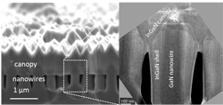 |
| Cross-sectional images of the indium gallium nitride nanowire solar cell. (Image courtesy of Sandia National Laboratories) |
Abstract:
Researchers creating electricity through photovoltaics want to convert as many of the sun's wavelengths as possible to achieve maximum efficiency. Otherwise, they're eating only a small part of a shot duck: wasting time and money by using only a tiny bit of the sun's incoming energies.
Solar nanowire array may increase percentage of sun's frequencies available for energy conversion: Sandia nanowire template permits flexible energy absorption
Albuquerque, NM | Posted on June 20th, 2012For this reason, they see indium gallium nitride as a valuable future material for photovoltaic systems. Changing the concentration of indium allows researchers to tune the material's response so it collects solar energy from a variety of wavelengths. The more variations designed into the system, the more of the solar spectrum can be absorbed, leading to increased solar cell efficiencies. Silicon, today's photovoltaic industry standard, is limited in the wavelength range it can 'see' and absorb.
But there is a problem: Indium gallium nitride, part of a family of materials called III-nitrides, is typically grown on thin films of gallium nitride. Because gallium nitride atomic layers have different crystal lattice spacings from indium gallium nitride atomic layers, the mismatch leads to structural strain that limits both the layer thickness and percentage of indium that can be added. Thus, increasing the percentage of indium added broadens the solar spectrum that can be collected, but reduces the material's ability to tolerate the strain.
Cross-sectional images of the indium gallium nitride nanowire solar cell. (Image courtesy of Sandia National Laboratories) Click on thumbnail for a high-resolution image.
Sandia National Laboratories scientists Jonathan Wierer Jr. and George Wang reported in the journal Nanotechnology that if the indium mixture is grown on a phalanx of nanowires rather than on a flat surface, the small surface areas of the nanowires allow the indium shell layer to partially "relax" along each wire, easing strain. This relaxation allowed the team to create a nanowire solar cell with indium percentages of roughly 33 percent, higher than any other reported attempt at creating III-nitride solar cells.
This initial attempt also lowered the absorption base energy from 2.4eV to 2.1 eV, the lowest of any III-nitride solar cell to date, and made a wider range of wavelengths available for power conversion. Power conversion efficiencies were low � only 0.3 percent compared to a standard commercial cell that hums along at about 15 percent � but the demonstration took place on imperfect nanowire-array templates. Refinements should lead to higher efficiencies and even lower energies.
Several unique techniques were used to create the III-nitride nanowire array solar cell. A top-down fabrication process was used to create the nanowire array by masking a gallium nitride (GaN) layer with a colloidal silica mask, followed by dry and wet etching. The resulting array consisted of nanowires with vertical sidewalls and of uniform height.
Next, shell layers containing the higher indium percentage of indium gallium nitride (InGaN) were formed on the GaN nanowire template via metal organic chemical vapor deposition. Lastly, In0.02Ga0.98N was grown, in such a way that caused the nanowires to coalescence. This process produced a canopy layer at the top, facilitating simple planar processing and making the technology manufacturable.
The results, says Wierer, although modest, represent a promising path forward for III-nitride solar cell research. The nano-architecture not only enables higher indium proportion in the InGaN layers but also increased absorption via light scattering in the faceted InGaN canopy layer, as well as air voids that guide light within the nanowire array.
The research was funded by DOE's Office of Science through the Solid State Lighting Science Energy Frontier Research Center, and Sandia's Laboratory Directed Research and Development program.
####
About DOE/Sandia National Laboratories
Sandia National Laboratories is a multi-program laboratory operated by Sandia Corporation, a wholly owned subsidiary of Lockheed Martin company, for the U.S. Department of Energy's National Nuclear Security Administration. With main facilities in Albuquerque, N.M., and Livermore, Calif., Sandia has major R&D responsibilities in national security, energy and environmental technologies and economic competitiveness.
For more information, please click here
Contacts:
Neal Singer
505-845-7078
Copyright © DOE/Sandia National Laboratories
If you have a comment, please Contact us.Issuers of news releases, not 7th Wave, Inc. or Nanotechnology Now, are solely responsible for the accuracy of the content.
Bookmark:


| Related News Press |
News and information
![]() Simulating magnetization in a Heisenberg quantum spin chain April 5th, 2024
Simulating magnetization in a Heisenberg quantum spin chain April 5th, 2024
![]() NRL charters Navy�s quantum inertial navigation path to reduce drift April 5th, 2024
NRL charters Navy�s quantum inertial navigation path to reduce drift April 5th, 2024
![]() Discovery points path to flash-like memory for storing qubits: Rice find could hasten development of nonvolatile quantum memory April 5th, 2024
Discovery points path to flash-like memory for storing qubits: Rice find could hasten development of nonvolatile quantum memory April 5th, 2024
Laboratories
![]() A battery�s hopping ions remember where they�ve been: Seen in atomic detail, the seemingly smooth flow of ions through a battery�s electrolyte is surprisingly complicated February 16th, 2024
A battery�s hopping ions remember where they�ve been: Seen in atomic detail, the seemingly smooth flow of ions through a battery�s electrolyte is surprisingly complicated February 16th, 2024
![]() NRL discovers two-dimensional waveguides February 16th, 2024
NRL discovers two-dimensional waveguides February 16th, 2024
![]() Three-pronged approach discerns qualities of quantum spin liquids November 17th, 2023
Three-pronged approach discerns qualities of quantum spin liquids November 17th, 2023
Govt.-Legislation/Regulation/Funding/Policy
![]() NRL charters Navy�s quantum inertial navigation path to reduce drift April 5th, 2024
NRL charters Navy�s quantum inertial navigation path to reduce drift April 5th, 2024
![]() Discovery points path to flash-like memory for storing qubits: Rice find could hasten development of nonvolatile quantum memory April 5th, 2024
Discovery points path to flash-like memory for storing qubits: Rice find could hasten development of nonvolatile quantum memory April 5th, 2024
![]() Chemical reactions can scramble quantum information as well as black holes April 5th, 2024
Chemical reactions can scramble quantum information as well as black holes April 5th, 2024
Discoveries
![]() Chemical reactions can scramble quantum information as well as black holes April 5th, 2024
Chemical reactions can scramble quantum information as well as black holes April 5th, 2024
![]() New micromaterial releases nanoparticles that selectively destroy cancer cells April 5th, 2024
New micromaterial releases nanoparticles that selectively destroy cancer cells April 5th, 2024
![]() Utilizing palladium for addressing contact issues of buried oxide thin film transistors April 5th, 2024
Utilizing palladium for addressing contact issues of buried oxide thin film transistors April 5th, 2024
Announcements
![]() NRL charters Navy�s quantum inertial navigation path to reduce drift April 5th, 2024
NRL charters Navy�s quantum inertial navigation path to reduce drift April 5th, 2024
![]() Discovery points path to flash-like memory for storing qubits: Rice find could hasten development of nonvolatile quantum memory April 5th, 2024
Discovery points path to flash-like memory for storing qubits: Rice find could hasten development of nonvolatile quantum memory April 5th, 2024
Energy
![]() Development of zinc oxide nanopagoda array photoelectrode: photoelectrochemical water-splitting hydrogen production January 12th, 2024
Development of zinc oxide nanopagoda array photoelectrode: photoelectrochemical water-splitting hydrogen production January 12th, 2024
![]() Shedding light on unique conduction mechanisms in a new type of perovskite oxide November 17th, 2023
Shedding light on unique conduction mechanisms in a new type of perovskite oxide November 17th, 2023
![]() Inverted perovskite solar cell breaks 25% efficiency record: Researchers improve cell efficiency using a combination of molecules to address different November 17th, 2023
Inverted perovskite solar cell breaks 25% efficiency record: Researchers improve cell efficiency using a combination of molecules to address different November 17th, 2023
![]() The efficient perovskite cells with a structured anti-reflective layer � another step towards commercialization on a wider scale October 6th, 2023
The efficient perovskite cells with a structured anti-reflective layer � another step towards commercialization on a wider scale October 6th, 2023
Solar/Photovoltaic
![]() Development of zinc oxide nanopagoda array photoelectrode: photoelectrochemical water-splitting hydrogen production January 12th, 2024
Development of zinc oxide nanopagoda array photoelectrode: photoelectrochemical water-splitting hydrogen production January 12th, 2024
![]() Shedding light on unique conduction mechanisms in a new type of perovskite oxide November 17th, 2023
Shedding light on unique conduction mechanisms in a new type of perovskite oxide November 17th, 2023
![]() Inverted perovskite solar cell breaks 25% efficiency record: Researchers improve cell efficiency using a combination of molecules to address different November 17th, 2023
Inverted perovskite solar cell breaks 25% efficiency record: Researchers improve cell efficiency using a combination of molecules to address different November 17th, 2023
![]() Charged �molecular beasts� the basis for new compounds: Researchers at Leipzig University use �aggressive� fragments of molecular ions for chemical synthesis November 3rd, 2023
Charged �molecular beasts� the basis for new compounds: Researchers at Leipzig University use �aggressive� fragments of molecular ions for chemical synthesis November 3rd, 2023
|
|
||
|
|
||
| The latest news from around the world, FREE | ||
|
|
||
|
|
||
| Premium Products | ||
|
|
||
|
Only the news you want to read!
Learn More |
||
|
|
||
|
Full-service, expert consulting
Learn More |
||
|
|
||