Home > Press > Sensing the infrared: Researchers improve IR detectors with single-walled carbon nanotubes: New design eliminates need for complex, expensive cooling systems
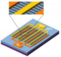 |
| This schematic shows the design of single-walled carbon nanotube photodetector, which provides a more efficient method of collecting infrared radiation without relying on cryogenics for cooling.
Credit: Image courtesy Sheng Wang, Peking University. |
Abstract:
Whether used in telescopes or optoelectronic communications, infrared detectors must be continuously cooled to avoid being overwhelmed by stray thermal radiation. Now, a team of researchers from Peking University, the Chinese Academy of Sciences, and Duke University (USA) is harnessing the remarkable properties of single-walled carbon nanotubes (SWNTs) to create highly sensitive, "uncooled" photovoltaic infrared detectors.
Sensing the infrared: Researchers improve IR detectors with single-walled carbon nanotubes: New design eliminates need for complex, expensive cooling systems
Washington, DC | Posted on May 23rd, 2012This new type of detector, which the team describes in a paper published today in the Optical Society's (OSA) open-access journal Optical Materials Express, may prove useful for industrial, military, manufacturing, optical communications, and scientific applications.
Carbon nanotubes are known for their outstanding mechanical, electrical, and optical properties. "They also are an ideal nanomaterial for infrared applications," says Sheng Wang, an associate professor in the Department of Electronics at Peking University in Beijing, China, and an author of the Optical Materials Express paper. "For starters, these nanotubes exhibit strong and broadband infrared light absorption, which can be tuned by selecting nanotubes of different diameters. Also, due to their high electron mobility, nanotubes react very rapidly - on the order of picoseconds - to infrared light." In comparison to traditional infrared detectors, which are based on semiconductors made of a mercury-cadmium-telluride alloy, the SWNTs are an order of magnitude more efficient, the researchers report.
The team's photovoltaic infrared detector is formed by aligning SWNT arrays on a silicon substrate. The nanotubes arrays are then placed between asymmetric palladium and scandium contacts. These two metals have properties that collectively create what is known as an Ohmic contact, a region in a semiconductor device that has very low electrical resistance, which helps make the detector operate more efficiently.
"Fabrication of carbon nanotube infrared detectors can be readily implemented on a flexible substrate and large wafer at a low cost," explains Wang.
The detector demonstrated "acceptable sensitivity" at room temperature and may be significantly improved by increasing the density of the carbon nanotubes, according to the team. The signal-to-noise performance of conventional infrared photodetectors is limited by their natural infrared emission, which is subsequently absorbed by the detector. To avoid having this stray radiation overwhelm the detector, liquid nitrogen or electric cooling is generally used to suppress this thermal effect. However, this makes infrared detectors more complex and expensive to operate. The new design eliminates this need because carbon nanotubes have special thermal properties. At room temperature, they emit comparatively little infrared radiation of their own, especially when the carbon nanotube is on the substrate. In addition, nanotubes are very good at conducting heat, so temperatures do not build up on the detector itself.
One of the biggest surprises for the team was achieving relatively high infrared detectivity (the radiation power required to produce a signal from a photoconductor) using a carbon nanotube thin film only a few nanometers thick, Wang points out. Notably, conventional infrared detectors require much thicker films, on the scale of hundreds of nanometers, to obtain comparable detectivity.
Another huge advantage of the detector is that the fabrication process is completely compatible with carbon nanotube transistors - meaning no big expensive equipment changes are necessary. "Our doping-free chemical approach provides an ideal platform for carbon nanotube electronic and optoelectronic integrated circuits," says Wang.
The next step for the team is to focus on improving the detectivity of the detector with greater SWNT density, and to also achieve a wide spectrum response with improved diameter control.
####
About Optical Society of America
Uniting more than 130,000 professionals from 175 countries, the Optical Society (OSA) brings together the global optics community through its programs and initiatives. Since 1916 OSA has worked to advance the common interests of the field, providing educational resources to the scientists, engineers and business leaders who work in the field by promoting the science of light and the advanced technologies made possible by optics and photonics. OSA publications, events, technical groups and programs foster optics knowledge and scientific collaboration among all those with an interest in optics and photonics. For more information, visit www.osa.org.
About Optical Materials Express
Optical Materials Express (OMEx) is OSA's newest peer-reviewed, open-access journal focusing on the synthesis, processing and characterization of materials for applications in optics and photonics. OMEx, which launched in April 2011, primarily emphasizes advances in novel optical materials, their properties, modeling, synthesis and fabrication techniques; how such materials contribute to novel optical behavior; and how they enable new or improved optical devices. For more information, visit www.OpticsInfoBase.org/OMEx.
For more information, please click here
Contacts:
Angela Stark
202-416-1443
Copyright © Optical Society of America
If you have a comment, please Contact us.Issuers of news releases, not 7th Wave, Inc. or Nanotechnology Now, are solely responsible for the accuracy of the content.
Bookmark:


| Related Links |
![]() The paper, "Carbon Nanotube Arrays Based High-Performance Infrared Photodetector,"by Q. Zeng et al.:
The paper, "Carbon Nanotube Arrays Based High-Performance Infrared Photodetector,"by Q. Zeng et al.:
| Related News Press |
News and information
![]() Quantum computer improves AI predictions April 17th, 2026
Quantum computer improves AI predictions April 17th, 2026
![]() Flexible sensor gains sensitivity under pressure April 17th, 2026
Flexible sensor gains sensitivity under pressure April 17th, 2026
![]() A reusable chip for particulate matter sensing April 17th, 2026
A reusable chip for particulate matter sensing April 17th, 2026
![]() Detecting vibrational quantum beating in the predissociation dynamics of SF6 using time-resolved photoelectron spectroscopy April 17th, 2026
Detecting vibrational quantum beating in the predissociation dynamics of SF6 using time-resolved photoelectron spectroscopy April 17th, 2026
Chip Technology
![]() A reusable chip for particulate matter sensing April 17th, 2026
A reusable chip for particulate matter sensing April 17th, 2026
![]() Metasurfaces smooth light to boost magnetic sensing precision January 30th, 2026
Metasurfaces smooth light to boost magnetic sensing precision January 30th, 2026
Nanotubes/Buckyballs/Fullerenes/Nanorods/Nanostrings/Nanosheets
![]() Tiny nanosheets, big leap: A new sensor detects ethanol at ultra-low levels January 30th, 2026
Tiny nanosheets, big leap: A new sensor detects ethanol at ultra-low levels January 30th, 2026
![]() Enhancing power factor of p- and n-type single-walled carbon nanotubes April 25th, 2025
Enhancing power factor of p- and n-type single-walled carbon nanotubes April 25th, 2025
![]() Chainmail-like material could be the future of armor: First 2D mechanically interlocked polymer exhibits exceptional flexibility and strength January 17th, 2025
Chainmail-like material could be the future of armor: First 2D mechanically interlocked polymer exhibits exceptional flexibility and strength January 17th, 2025
![]() Innovative biomimetic superhydrophobic coating combines repair and buffering properties for superior anti-erosion December 13th, 2024
Innovative biomimetic superhydrophobic coating combines repair and buffering properties for superior anti-erosion December 13th, 2024
Sensors
![]() Flexible sensor gains sensitivity under pressure April 17th, 2026
Flexible sensor gains sensitivity under pressure April 17th, 2026
![]() Tiny nanosheets, big leap: A new sensor detects ethanol at ultra-low levels January 30th, 2026
Tiny nanosheets, big leap: A new sensor detects ethanol at ultra-low levels January 30th, 2026
![]() From sensors to smart systems: the rise of AI-driven photonic noses January 30th, 2026
From sensors to smart systems: the rise of AI-driven photonic noses January 30th, 2026
![]() Sensors innovations for smart lithium-based batteries: advancements, opportunities, and potential challenges August 8th, 2025
Sensors innovations for smart lithium-based batteries: advancements, opportunities, and potential challenges August 8th, 2025
Discoveries
![]() Quantum computer improves AI predictions April 17th, 2026
Quantum computer improves AI predictions April 17th, 2026
![]() Flexible sensor gains sensitivity under pressure April 17th, 2026
Flexible sensor gains sensitivity under pressure April 17th, 2026
![]() A reusable chip for particulate matter sensing April 17th, 2026
A reusable chip for particulate matter sensing April 17th, 2026
![]() Detecting vibrational quantum beating in the predissociation dynamics of SF6 using time-resolved photoelectron spectroscopy April 17th, 2026
Detecting vibrational quantum beating in the predissociation dynamics of SF6 using time-resolved photoelectron spectroscopy April 17th, 2026
Announcements
![]() A fundamentally new therapeutic approach to cystic fibrosis: Nanobody repairs cellular defect April 17th, 2026
A fundamentally new therapeutic approach to cystic fibrosis: Nanobody repairs cellular defect April 17th, 2026
![]() UC Irvine physicists discover method to reverse �quantum scrambling� : The work addresses the problem of information loss in quantum computing system April 17th, 2026
UC Irvine physicists discover method to reverse �quantum scrambling� : The work addresses the problem of information loss in quantum computing system April 17th, 2026
Energy
![]() Sensors innovations for smart lithium-based batteries: advancements, opportunities, and potential challenges August 8th, 2025
Sensors innovations for smart lithium-based batteries: advancements, opportunities, and potential challenges August 8th, 2025
![]() Simple algorithm paired with standard imaging tool could predict failure in lithium metal batteries August 8th, 2025
Simple algorithm paired with standard imaging tool could predict failure in lithium metal batteries August 8th, 2025
Solar/Photovoltaic
![]() Spinel-type sulfide semiconductors to operate the next-generation LEDs and solar cells For solar-cell absorbers and green-LED source October 3rd, 2025
Spinel-type sulfide semiconductors to operate the next-generation LEDs and solar cells For solar-cell absorbers and green-LED source October 3rd, 2025
![]() KAIST researchers introduce new and improved, next-generation perovskite solar cell November 8th, 2024
KAIST researchers introduce new and improved, next-generation perovskite solar cell November 8th, 2024
![]() Groundbreaking precision in single-molecule optoelectronics August 16th, 2024
Groundbreaking precision in single-molecule optoelectronics August 16th, 2024
![]() Development of zinc oxide nanopagoda array photoelectrode: photoelectrochemical water-splitting hydrogen production January 12th, 2024
Development of zinc oxide nanopagoda array photoelectrode: photoelectrochemical water-splitting hydrogen production January 12th, 2024
|
|
||
|
|
||
| The latest news from around the world, FREE | ||
|
|
||
|
|
||
| Premium Products | ||
|
|
||
|
Only the news you want to read!
Learn More |
||
|
|
||
|
Full-service, expert consulting
Learn More |
||
|
|
||