Home > Press > Printing with Lasers: Making Electronics Quick and Easy
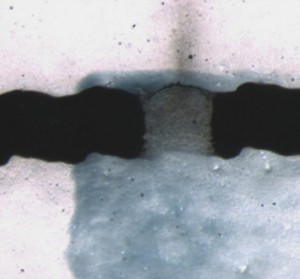 |
| An optical microscopy image on of the channels in a printed OECT array. |
Abstract:
The field of printed electronics has given us a vision of ubiquitous electronic products, integrated on everyday, low-cost products, such as sensors or labels that can be printed on flexible substrates for food packages to indicate fresheness, temperature, or other important parameters. However, printing of electronic devices requires a resolution that is beyond the limit of conventional graphical printing. Another bottleneck that prevents production scale-up (e.g. roll-to-roll or sheet-based manufacturing) is the accuracy of the positioning of the substrate between the individual process steps.
Printing with Lasers: Making Electronics Quick and Easy
Germany | Posted on May 17th, 2012Now, in new work, a German-Swedish research collaboration between the Chemnitz University of Technology, the Fraunhofer Institute of Electronic Nanosystems (Chemnitz), Link�ping University, and Acreo AB (Norrk�ping, a research institute from the Swedish ICT sector), present a novel, hybrid manufacturing concept for organic electrochemical transistors (OECTs).
Initiated by the EU ICT FP7 Network of Excellence "PolyNet" (2008-2010, grant agreement 214006), the researchers combined standard printing and laser microstructuring techniques. The nice thing with OECTs is that their electrical parameters do not strictly relate to the feature size: low-voltage operation is independent of the transistor channel length and the thickness of the dielectric layer, lowering the resolution demands compared to other transistor concepts like field-effect transistors.
Addressing the alignment precision, the key of the manufacturing concept is to have the laser light find its target automatically: only when and where the scanning laser hits the printed conductive layer, the material is delaminated and the layer is separated into the two electrodes, source and drain. At the same time, the deposited heat introduces a vertical void in the transparent dielectric layer above. The void is autonomously filled by capillary forces when applying a semiconductor material in a subsequent printing step. Finally, after printing a liquid electrolyte, a coated plastic foil is laminated on the stack from the top, forming the gate electrode and completing the transistor.
The subtractive step allows for printing arrays of OECTs (17�50) on DIN A4 (297�210 mm�) flexible sheet substrates. As a perspective, the combined usage of digital techniques (scanning laser, inkjet printing) can pave the way for personalized devices, e.g. arrays of OECTs with varying electrolytes as the active elements in printed large-area sensor arrays.
####
For more information, please click here
Copyright © Wiley-VCH Materials Science Journals
If you have a comment, please Contact us.Issuers of news releases, not 7th Wave, Inc. or Nanotechnology Now, are solely responsible for the accuracy of the content.
Bookmark:


| Related Links |
![]() Link to the original paper on Wiley Online Library:
Link to the original paper on Wiley Online Library:
| Related News Press |
News and information
![]() Quantum computer improves AI predictions April 17th, 2026
Quantum computer improves AI predictions April 17th, 2026
![]() Flexible sensor gains sensitivity under pressure April 17th, 2026
Flexible sensor gains sensitivity under pressure April 17th, 2026
![]() A reusable chip for particulate matter sensing April 17th, 2026
A reusable chip for particulate matter sensing April 17th, 2026
![]() Detecting vibrational quantum beating in the predissociation dynamics of SF6 using time-resolved photoelectron spectroscopy April 17th, 2026
Detecting vibrational quantum beating in the predissociation dynamics of SF6 using time-resolved photoelectron spectroscopy April 17th, 2026
Discoveries
![]() Quantum computer improves AI predictions April 17th, 2026
Quantum computer improves AI predictions April 17th, 2026
![]() Flexible sensor gains sensitivity under pressure April 17th, 2026
Flexible sensor gains sensitivity under pressure April 17th, 2026
![]() A reusable chip for particulate matter sensing April 17th, 2026
A reusable chip for particulate matter sensing April 17th, 2026
![]() Detecting vibrational quantum beating in the predissociation dynamics of SF6 using time-resolved photoelectron spectroscopy April 17th, 2026
Detecting vibrational quantum beating in the predissociation dynamics of SF6 using time-resolved photoelectron spectroscopy April 17th, 2026
Announcements
![]() A fundamentally new therapeutic approach to cystic fibrosis: Nanobody repairs cellular defect April 17th, 2026
A fundamentally new therapeutic approach to cystic fibrosis: Nanobody repairs cellular defect April 17th, 2026
![]() UC Irvine physicists discover method to reverse �quantum scrambling� : The work addresses the problem of information loss in quantum computing system April 17th, 2026
UC Irvine physicists discover method to reverse �quantum scrambling� : The work addresses the problem of information loss in quantum computing system April 17th, 2026
Printing/Lithography/Inkjet/Inks/Bio-printing/Dyes
![]() Presenting: Ultrasound-based printing of 3D materials�potentially inside the body December 8th, 2023
Presenting: Ultrasound-based printing of 3D materials�potentially inside the body December 8th, 2023
![]() Simple ballpoint pen can write custom LEDs August 11th, 2023
Simple ballpoint pen can write custom LEDs August 11th, 2023
![]() Disposable electronics on a simple sheet of paper October 7th, 2022
Disposable electronics on a simple sheet of paper October 7th, 2022
|
|
||
|
|
||
| The latest news from around the world, FREE | ||
|
|
||
|
|
||
| Premium Products | ||
|
|
||
|
Only the news you want to read!
Learn More |
||
|
|
||
|
Full-service, expert consulting
Learn More |
||
|
|
||