Home > Press > The microstructure of multi-layerĀnc-CaĀfilms on different substrates
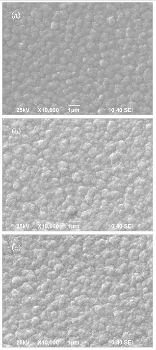 |
| Fig. 4 SEM images of the MgF2 on different substrates: (a) CaF2, (b) Si(100), (c) Si(111). |
Abstract:
Multi-layerĀnanocrystalline Ca (nc-Ca)Āfilms were prepared by vacuum evaporation method, using of three different material as the substrate, including of CaF2, Si(100), Si(111). The films at room temperature, can be stored in the air for a long time, and there was no obvious shedding phenomenon. Nc-ca thin films on different substrates were characterized by XRD analysis, obtained (111) preferred orientation of the conclusions. The average grain size of the Ca was 36.8nm on the CaF2 substrate, and the average grain size of the Ca was 43.9nm on the Si(100) substrate. By the SEM analysis, there was a better surface morphology of the films on the CaF2 substrate.
The microstructure of multi-layerĀnc-CaĀfilms on different substrates
Xinxiang, PR China | Posted on April 4th, 2012Introduction
Recently, with the development of thin films technology, various properties of thin films in optical devices, optoelectronic devices and optical communication applications have been very common[1-4]. Two-dimensional morphology of the thin films, which are different from the bulk material, have played an irreplaceable role for the device in thin short and system integration. Because different materials have different physical and chemical properties, so that workers who engaged in materials science have done a very extensive research, especially in some of the physical and chemical properties stability materials in the mostly, such as Si, Al, ZnO, there are a lot of literature are reported[5-10]. However, for some lively physical and chemical properties materials, the preparation of thin films are difficult, the materials are hard to preserve, so some of the materials in the actual application are often subject to certain restrictions. In this article, as the primary coating composition, Ca elemental material is easy to be deliquesced and oxidized in the air[11-12], so the preparation of monolayer Ca films are difficult to achieve, and there need other material to be deposited on the Ca films as protective layer. In the experiment ,we chose MgF2 as the outermost layer for protection, and chose CaF2 as the middle for the transition layer. Eventually a multi-layer nc-Ca films with more stable physical and chemical properties had been preparation. Through the XRD and SEM analysis for the resultant films on different substrates, respectively, it was obtained the average gain size of Ca, the preferred orientation of the crystal surface as well as some of the information of the surface morphology of the outermost layer of MgF2. These for further understanding of the nature of the Ca films, how to deposited the physical and chemical properties more excellent Ca films will play a certain help.
1 Experimental procedure
Experiments using DM-7H44700-7 type optical vacuum coating machine, taked φ40ū0.38mm of Si(111) and Si(100), as well asφ15ū0.3mm of CaF2 as the substrate, respectively. Table 1 shows the multilayer structure of the thin films. The experiment used Ca and MgF2 were 99.99% purity, CaF2 was the pure spectrum.
A
MgF2
CaF2
Ca
CaF2
Ca
CaF2
Ca
CaF2
Ca
CaF2
Ca
S
Geometric thickness(nm)
200
100
30
100
50
100
50
100
100
100
300
Table. 1 The multilayer structure of the thin films
Prior to depositing the thin film, the diffusion pump should be preheated for 40-50 minutes, then using the mechanical pump and diffusion pump to vacuumize the vacuum chamber to 4.0ū10-3Pa, and controllingĀthe substrate temperatureĀwasĀmaintainedĀat 200Ā░ C.
There used electron beam evaporation deposition of Ca and MgF2 films, because CaF2 was fine power, the electron beam could generate splash, so the way for the CaF2 used the thermal resistance evaporation. The deposition rate controlled at 0.8-1.1nm/s. The beginning of evaporation, the beginning of evaporation, the pressure down to 2.6ū103Pa, indicating that the residual gas of the vacuum chamber should be absorbed a small amount by Ca films. With the evaporation progresses, the vacuum chamber pressure stabilized at 3.6ū10-3Pa. After completion of films deposition, all the films were annealed at 200░ C for 30 minutes. Finally the thickness of the films were 1233.8nm, there was about 3.8nm error between the actual films thickness and the design films thickness. The films at room temperature, can be stored in the air for a long time, and there was no obvious shedding phenomenon.
2 Results and Discussion
2.1 XRD analysis
Figure 1 shows the XRD patterns of the multilayer nc-Ca films, using the CaF2 as the substrate. Multilayer nc-Ca films existence of Ca(111) and Ca(200) two crystal faces can be seen from the diffraction lines, showing the polycrystalline structure. The Ca(111) crystal face diffraction intensity is stronger than the Ca(200) crystal face diffraction intensity, and better preferred orientation in the Ca(111) crystal face, which the full width at half maximun (FWHM) is 0.233 degree. According to the formula:
Where: d is the average grain size; k is the constant equal to 0.94; λ is the wavelength of X-ray equal to 0.154nm; b is the FWHM of the diffraction peak; θ is the diffraction angle. The average grain size of Ca can be calculated is 36.8nm.
Figure 2 shows the XRD patterns of the multilayer nc-Ca films, using the Si(100) as the substrate. There can be seen from the figure of Ca films which are still showing a polycrystalline structure, and choose a different substrate, resulting in Ca in two crystal diffraction intensity have increased, but the films are still Ca(111) preferred orientation. There can also be obtained the FWHM is 0.199 degree, the average grain size is 43.9nm.
Figure 3 shows the XRD patterns of the multilayer Ca films, using the Si(111) as the substrate. Due to the influence of the substrate lattice, the crystal face diffraction peak of the CaF2(111) is strengthened, covering on the point of view of the nearby diffraction peaks. In order to qualitatively analyze the strength of other diffraction peaks, here will be part of the amplification in figure 3, the (b) is the image 34 degree to 70 degree of (a) in figure 3, it can be found the crystal face diffraction intensity of the CaO(200) and CaF2(220), respectively, is stronger than the situation which using CaF2 and Si(100) as a substrate.
It is generally believed that the preferred orientation factors affect the films there are two main aspects. On the one hand, it is the nature of the films itself, namely the nucleation ability which nucleation growth along different crystal planes, and the nucleation growth rate. On the other hand, the factor is determined by external conditions, such as heat treatment, substrate temperature, and lattice mismatch. According to the information in the PDF card. In Ca films, the interplanar spacing of (111) is 0.324nm, the interplanar spacing of (200) is 0.28nm. In CaF2 films, the interplanar spacing of (111) is 0.312nm. In Si films, the interplanar spacing of (111) is 0.311nm, and the interplanar spacing of (100) is 0.237nm. Depending on the size of the lattice matching, the surface mismatch between Ca(111) and CaF2(111) is 3.8%, and the surface mismatch between Ca(111) and Si(111) is 4.1%, so it is easily (111) preferred orientation in the films which using CaF2 and Si(111) as the substrate. On the Si(100) substrate, because the interplanar spacing of Ca(200) is closer to the interplanar spacing of Si(100), so in Figure 2, Ca(200) crystal face appear the fast-growing phenomenon, but still (111) preferred orientation.
2.2 SEM analysis
Figure 4 shows the SEM images of the MgF2 surface on different substrates: (a) CaF2, (b) Si(100), (c) Si(111). There can be observed form the image (a), the grains, which are intact, neat and having uniform size and regular geometric crystal surface, are distributed in the scanning range, and the grain boundary is obvious, the lateral dimensions of grains is less than 1μm. Compared with (a), the surface morphology of image (b) and (c) are relatively rough, the grain size is non-uniform, and the lateral dimensions of grains is between 1μm to 0.3μm.
The main factors determining the surface morphology of thin film are the nucleation and growth mode. The flatness of the substrate surface, make defects and dislocations as the initial nucleation steps of thin films growth. The films began to grow in these steps, with relatively complete crystallization, the orientation of this layer of the films is strictly subject to the constraint of the substrate. This constraint is gradually weakened with increasing film thickness. However, due to the increase of the film layers, the effect of crystal orientation cumulative to the film surface, finally, the surface morphology of Figure 4 is more effective than the surface morphology of Figure 5 and Figure 6.
3 Conclusion
This paper had discussed the experimental process of the preparation of the multiple nc-Ca films on three different substrates. The resultant films at room temperature, can be stored in the air for a long time, and there was no obvious shedding phenomenon. In such a prerequisite, the XRD analysis of the films showed Ca film (111) preferred orientation on three different substrates. By measuring the FWHM value, there were calculated the average grain size of Ca was 36.8nm and 43.9nm on CaF2 substrate and Si(100) substrate, respectively. By the SEM analysis of MgF2 surface, it was found that a better surface morphology of the film on the CaF2 substrate.
References:
1 Tadatsugu Minami. Thin Solid Films, 2008, 516: 5822-5828.
2 Martin A.Green. Solar Energy, 2003, 74: 181-192.
3 Franz H.Karg. Solar Energy Materials & Solar Cells, 2001, 66: 645-653.
4 Neelkanth G.Dhere. Solar Energy Materials & Solar Cells, 2006, 90: 2181-2190.
5 Shoji Nishida, Katsumi Nakagawa, Masaaki Iwane, et al. Solar Energy Materials & Solar Cells, 2001, 65: 525-532.
6 Byeong Yeon Moon, Jae Hyoung Youn, Sung Hwan Won, et al. Solar Energy Materials & Solar Cells, 2001, 69: 139-145.
7 D.Herrmann, M.Oertel, R.Menner, et al. Surface and Coatings Technology, 2003, 174: 229-234.
####
About Henan Normal University
Henan Normal University is one of the key universities directly under the provincial government, developed from the Zhongzhou University (founded in 1923) and Pingyuan Teachers college (founded in 1951). It is situated in Xinxiang, a famous city in north Henan, which is at the junction of the Beijing- Guangzhou, Taiyuan-Heze railways, nestling near Taihang Mountain to the north and the Yellow River to the south, where the famous Muye battle once took place. Due to the adjustment of colleges and departments, the university has successfully been renamed as Henan Teachers College 2, Henan Second Teachers college and Xinxiang Teachers College after the founding of New China. And in 1985, she began to be called Henan Normal University.
For more information, please click here
Contacts:
De-wen Meng
Copyright © Henan Normal University
If you have a comment, please Contact us.Issuers of news releases, not 7th Wave, Inc. or Nanotechnology Now, are solely responsible for the accuracy of the content.
Bookmark:


| Related News Press |
News and information
![]() Quantum computer improves AI predictions April 17th, 2026
Quantum computer improves AI predictions April 17th, 2026
![]() Flexible sensor gains sensitivity under pressure April 17th, 2026
Flexible sensor gains sensitivity under pressure April 17th, 2026
![]() A reusable chip for particulate matter sensing April 17th, 2026
A reusable chip for particulate matter sensing April 17th, 2026
![]() Detecting vibrational quantum beating in the predissociation dynamics of SF6 using time-resolved photoelectron spectroscopy April 17th, 2026
Detecting vibrational quantum beating in the predissociation dynamics of SF6 using time-resolved photoelectron spectroscopy April 17th, 2026
Chip Technology
![]() A reusable chip for particulate matter sensing April 17th, 2026
A reusable chip for particulate matter sensing April 17th, 2026
![]() Metasurfaces smooth light to boost magnetic sensing precision January 30th, 2026
Metasurfaces smooth light to boost magnetic sensing precision January 30th, 2026
Discoveries
![]() Quantum computer improves AI predictions April 17th, 2026
Quantum computer improves AI predictions April 17th, 2026
![]() Flexible sensor gains sensitivity under pressure April 17th, 2026
Flexible sensor gains sensitivity under pressure April 17th, 2026
![]() A reusable chip for particulate matter sensing April 17th, 2026
A reusable chip for particulate matter sensing April 17th, 2026
![]() Detecting vibrational quantum beating in the predissociation dynamics of SF6 using time-resolved photoelectron spectroscopy April 17th, 2026
Detecting vibrational quantum beating in the predissociation dynamics of SF6 using time-resolved photoelectron spectroscopy April 17th, 2026
Announcements
![]() A fundamentally new therapeutic approach to cystic fibrosis: Nanobody repairs cellular defect April 17th, 2026
A fundamentally new therapeutic approach to cystic fibrosis: Nanobody repairs cellular defect April 17th, 2026
![]() UC Irvine physicists discover method to reverse æquantum scramblingÆ : The work addresses the problem of information loss in quantum computing system April 17th, 2026
UC Irvine physicists discover method to reverse æquantum scramblingÆ : The work addresses the problem of information loss in quantum computing system April 17th, 2026
|
|
||
|
|
||
| The latest news from around the world, FREE | ||
|
|
||
|
|
||
| Premium Products | ||
|
|
||
|
Only the news you want to read!
Learn More |
||
|
|
||
|
Full-service, expert consulting
Learn More |
||
|
|
||