Home > Press > Nanoscale magnetic media diagnostics by rippling spin waves
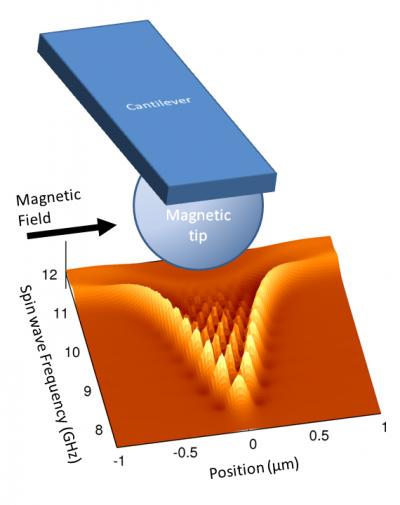 |
| Trapped beneath the magnetic tip of a microscale cantilever, spin waves can be used to non-destructively measure the properties of magnetic materials and search for nanoscale defects, especially in multilayer magnetic systems like a typical hard drive, where defects could be buried beneath the surface.
Credit: McMichael/NIST |
Abstract:
Memory devices based on magnetism are one of the core technologies of the computing industry, and engineers are working to develop new forms of magnetic memory that are faster, smaller, and more energy efficient than today's flash and SDRAM memory. They now have a new tool developed by a team from the National Institute of Standards and Technology (NIST), the University of Maryland Nanocenter and the Royal Institute of Technology in Sweden—a method to detect defects in magnetic structures as small as a tenth of a micrometer even if the region in question is buried inside a multilayer electronic device.*
Nanoscale magnetic media diagnostics by rippling spin waves
Gaithersburg, MD | Posted on April 3rd, 2012The technique demonstrated at the NIST Center for Nanoscale Technology (CNST) builds on work by researchers at the Ohio State University.** The idea is to trap and image oscillating perturbations of a magnetic field—"spin waves"—in a thin film. Trapped spin waves provide scientists with a powerful new tool to nondestructively measure the properties of magnetic materials and search for nanoscale defects that could or have caused memory failures, especially in multilayer magnetic systems like a typical hard drive, where defects could be buried beneath the surface.
According to NIST researcher Robert McMichael, when left alone, the material's magnetization is like the surface of a pond on a windless day. The pond is comprised of smaller magnetic moments that come with the quantum mechanical "spin" of electrons. Tap the surface of the pond with a piece of driftwood, or microwaves in this case, and the surface will begin to ripple with spin waves as the microwave energy jostles the spins, which, in turn, jostle their neighbors.
"The trick we play is to tune the microwaves to a frequency just outside the band where the spin waves can propagate—except right under our magnetic probe tip," says McMichael. "It's like the pond is frozen except for a little melted spot that we can move around to check magnetic properties at different spots in the sample."
The trapped spin waves are disturbed by defects in the material, and this effect allows the defects to be characterized on 100 nm length scales.
Previous work had shown this same effect in magnetic spins that were oriented perpendicular to the magnetic film surface, meaning that the individual spins coupled strongly with their neighbors, which limited the resolution. This new work adds the extra feature that the magnetic spins are aligned in plane with one another and are not as tightly coupled. This setup is not only more representative of how many magnetic devices would be structured, but also allows for tighter focusing and better resolution.
* H-J. Chia, F. Guo, L.M. Belova and R. D. McMichael. Nanoscale spin wave localization using ferromagnetic resonance force microscopy. Physical Review Letters. 108, 087206 (2012). prl.aps.org/pdf/PRL/v108/i8/e087206.
** See Lee et al. Nanoscale scanning probe ferromagnetic resonance imaging using localized modes. Nature. 466, 12. Aug. 12, 2010. doi:10.1038/nature09279.
####
For more information, please click here
Contacts:
Mark Esser,
301-975-8735
Copyright © National Institute of Standards and Technology (NIST)
If you have a comment, please Contact us.Issuers of news releases, not 7th Wave, Inc. or Nanotechnology Now, are solely responsible for the accuracy of the content.
Bookmark:


| Related News Press |
News and information
![]() Quantum computer improves AI predictions April 17th, 2026
Quantum computer improves AI predictions April 17th, 2026
![]() Flexible sensor gains sensitivity under pressure April 17th, 2026
Flexible sensor gains sensitivity under pressure April 17th, 2026
![]() A reusable chip for particulate matter sensing April 17th, 2026
A reusable chip for particulate matter sensing April 17th, 2026
![]() Detecting vibrational quantum beating in the predissociation dynamics of SF6 using time-resolved photoelectron spectroscopy April 17th, 2026
Detecting vibrational quantum beating in the predissociation dynamics of SF6 using time-resolved photoelectron spectroscopy April 17th, 2026
Thin films
![]() Tiny nanosheets, big leap: A new sensor detects ethanol at ultra-low levels January 30th, 2026
Tiny nanosheets, big leap: A new sensor detects ethanol at ultra-low levels January 30th, 2026
![]() Utilizing palladium for addressing contact issues of buried oxide thin film transistors April 5th, 2024
Utilizing palladium for addressing contact issues of buried oxide thin film transistors April 5th, 2024
Laboratories
![]() Researchers develop molecular qubits that communicate at telecom frequencies October 3rd, 2025
Researchers develop molecular qubits that communicate at telecom frequencies October 3rd, 2025
Govt.-Legislation/Regulation/Funding/Policy
![]() Quantum computer improves AI predictions April 17th, 2026
Quantum computer improves AI predictions April 17th, 2026
![]() Metasurfaces smooth light to boost magnetic sensing precision January 30th, 2026
Metasurfaces smooth light to boost magnetic sensing precision January 30th, 2026
![]() New imaging approach transforms study of bacterial biofilms August 8th, 2025
New imaging approach transforms study of bacterial biofilms August 8th, 2025
Memory Technology
![]() Researchers tackle the memory bottleneck stalling quantum computing October 3rd, 2025
Researchers tackle the memory bottleneck stalling quantum computing October 3rd, 2025
![]() First real-time observation of two-dimensional melting process: Researchers at Mainz University unveil new insights into magnetic vortex structures August 8th, 2025
First real-time observation of two-dimensional melting process: Researchers at Mainz University unveil new insights into magnetic vortex structures August 8th, 2025
![]() Utilizing palladium for addressing contact issues of buried oxide thin film transistors April 5th, 2024
Utilizing palladium for addressing contact issues of buried oxide thin film transistors April 5th, 2024
Discoveries
![]() Quantum computer improves AI predictions April 17th, 2026
Quantum computer improves AI predictions April 17th, 2026
![]() Flexible sensor gains sensitivity under pressure April 17th, 2026
Flexible sensor gains sensitivity under pressure April 17th, 2026
![]() A reusable chip for particulate matter sensing April 17th, 2026
A reusable chip for particulate matter sensing April 17th, 2026
![]() Detecting vibrational quantum beating in the predissociation dynamics of SF6 using time-resolved photoelectron spectroscopy April 17th, 2026
Detecting vibrational quantum beating in the predissociation dynamics of SF6 using time-resolved photoelectron spectroscopy April 17th, 2026
Announcements
![]() A fundamentally new therapeutic approach to cystic fibrosis: Nanobody repairs cellular defect April 17th, 2026
A fundamentally new therapeutic approach to cystic fibrosis: Nanobody repairs cellular defect April 17th, 2026
![]() UC Irvine physicists discover method to reverse ‘quantum scrambling’ : The work addresses the problem of information loss in quantum computing system April 17th, 2026
UC Irvine physicists discover method to reverse ‘quantum scrambling’ : The work addresses the problem of information loss in quantum computing system April 17th, 2026
|
|
||
|
|
||
| The latest news from around the world, FREE | ||
|
|
||
|
|
||
| Premium Products | ||
|
|
||
|
Only the news you want to read!
Learn More |
||
|
|
||
|
Full-service, expert consulting
Learn More |
||
|
|
||