Home > Press > New technique to detect and manipulate nano-objects using plasmonic nano-cavities
 |
| OpticalTrapping: SIBA plasmonic trapping using a Fabry�P�rot nanopore cavity |
Abstract:
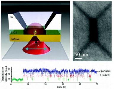
Imec researchers have presented a new approach to detect and manipulate nano-objects. The technique makes use of plasmonic excitation in nanocavities. In a demonstration, a rectangular nanocavity was used to detect the presence of 22nm beads. This approach may open new routes to create optical tweezers at the nanoscale, for ultra-accurate sensing, trapping, and arranging of nanoscale objects, such as biomolecules (e.g. proteins or DNA).
New technique to detect and manipulate nano-objects using plasmonic nano-cavities
Leuven, Belgium | Posted on March 16th, 2012Optical trapping techniques, the so called optical tweezers, are used to trap and manipulate objects. A highly focused laser beam provides an attractive or repulsive force to physically hold and move microscopic dielectric objects (down to micrometer-scale). But this technique cannot be applied straightforward to nanoscale objects. The energy required to manipulate such small objects is simply too large in relation to their size and would destroy the objects. Recently, researchers have therefore come up with the idea to make use of the strong local fields of metal nanostructures that are excited by light.
When metal nanostructures are illuminated with visible to near-infrared light, strong local electromagnetic fields are generated. These are caused by the collective oscillations of conduction electrons - called surface plasmons. These fields can be detected and visualized e.g. through surface-enhanced Raman spectroscopy. And because the presence of nanosized objects, such as biomulecules, causes changes in the fields, this phenomenon can be used as a sensor.
But the energy of the local fields could also be used to trap and manipulate the nanosized objects. In a recent publication, imec's researchers now present a new approach that uses this technique. They combine self-induced back action (SIBA) trapping with the latest advances in nanoscale plasmon engineering.
As a demonstration, the researchers designed a resonant trap in the form of a rectangular nanopore. This form of pore allows for tuning the plamons by changing the aspect ratio. This trap was successfully tested with 22nm polystyrene beads, distinguishing between events where one bead was trapped, or those where two beads were trapped at the same time. As part of their work, the researchers also proposed a figure of merit to quantify the efficiency of their trapping mechanism and to compare it to other optical nanotweezers.
####
For more information, please click here
Contacts:
Barbara Kalkis
Maestro Marketing & PR
Copyright © IMEC
If you have a comment, please Contact us.Issuers of news releases, not 7th Wave, Inc. or Nanotechnology Now, are solely responsible for the accuracy of the content.
Bookmark:


| Related Links |
![]() This work was published in the January edition of Nano-letters:
This work was published in the January edition of Nano-letters:
| Related News Press |
News and information
![]() Quantum computer improves AI predictions April 17th, 2026
Quantum computer improves AI predictions April 17th, 2026
![]() Flexible sensor gains sensitivity under pressure April 17th, 2026
Flexible sensor gains sensitivity under pressure April 17th, 2026
![]() A reusable chip for particulate matter sensing April 17th, 2026
A reusable chip for particulate matter sensing April 17th, 2026
![]() Detecting vibrational quantum beating in the predissociation dynamics of SF6 using time-resolved photoelectron spectroscopy April 17th, 2026
Detecting vibrational quantum beating in the predissociation dynamics of SF6 using time-resolved photoelectron spectroscopy April 17th, 2026
Sensors
![]() Flexible sensor gains sensitivity under pressure April 17th, 2026
Flexible sensor gains sensitivity under pressure April 17th, 2026
![]() Tiny nanosheets, big leap: A new sensor detects ethanol at ultra-low levels January 30th, 2026
Tiny nanosheets, big leap: A new sensor detects ethanol at ultra-low levels January 30th, 2026
![]() From sensors to smart systems: the rise of AI-driven photonic noses January 30th, 2026
From sensors to smart systems: the rise of AI-driven photonic noses January 30th, 2026
![]() Sensors innovations for smart lithium-based batteries: advancements, opportunities, and potential challenges August 8th, 2025
Sensors innovations for smart lithium-based batteries: advancements, opportunities, and potential challenges August 8th, 2025
Discoveries
![]() Quantum computer improves AI predictions April 17th, 2026
Quantum computer improves AI predictions April 17th, 2026
![]() Flexible sensor gains sensitivity under pressure April 17th, 2026
Flexible sensor gains sensitivity under pressure April 17th, 2026
![]() A reusable chip for particulate matter sensing April 17th, 2026
A reusable chip for particulate matter sensing April 17th, 2026
![]() Detecting vibrational quantum beating in the predissociation dynamics of SF6 using time-resolved photoelectron spectroscopy April 17th, 2026
Detecting vibrational quantum beating in the predissociation dynamics of SF6 using time-resolved photoelectron spectroscopy April 17th, 2026
Announcements
![]() A fundamentally new therapeutic approach to cystic fibrosis: Nanobody repairs cellular defect April 17th, 2026
A fundamentally new therapeutic approach to cystic fibrosis: Nanobody repairs cellular defect April 17th, 2026
![]() UC Irvine physicists discover method to reverse �quantum scrambling� : The work addresses the problem of information loss in quantum computing system April 17th, 2026
UC Irvine physicists discover method to reverse �quantum scrambling� : The work addresses the problem of information loss in quantum computing system April 17th, 2026
Tools
![]() Metasurfaces smooth light to boost magnetic sensing precision January 30th, 2026
Metasurfaces smooth light to boost magnetic sensing precision January 30th, 2026
![]() From sensors to smart systems: the rise of AI-driven photonic noses January 30th, 2026
From sensors to smart systems: the rise of AI-driven photonic noses January 30th, 2026
![]() Japan launches fully domestically produced quantum computer: Expo visitors to experience quantum computing firsthand August 8th, 2025
Japan launches fully domestically produced quantum computer: Expo visitors to experience quantum computing firsthand August 8th, 2025
Alliances/Trade associations/Partnerships/Distributorships
![]() Chicago Quantum Exchange welcomes six new partners highlighting quantum technology solutions, from Chicago and beyond September 23rd, 2022
Chicago Quantum Exchange welcomes six new partners highlighting quantum technology solutions, from Chicago and beyond September 23rd, 2022
![]() University of Illinois Chicago joins Brookhaven Lab's Quantum Center June 10th, 2022
University of Illinois Chicago joins Brookhaven Lab's Quantum Center June 10th, 2022
|
|
||
|
|
||
| The latest news from around the world, FREE | ||
|
|
||
|
|
||
| Premium Products | ||
|
|
||
|
Only the news you want to read!
Learn More |
||
|
|
||
|
Full-service, expert consulting
Learn More |
||
|
|
||