Home > Press > Eureka! Kitchen gadget inspires scientist to make more effective plastic electronics
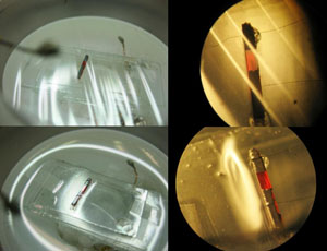 |
| Credit: H. T. Yi, et. al.
Fabricating single crystal organic field-effect transistors using ultra-thin polymer membrane for a gate insulator. In the upper row, the membrane is stretched over the transistor before vacuum is applied. In the lower row, the vacuum has been applied and the membrant is adhering to the organic crystal. Photos on the right are close-up views of the transistor, with the organic semiconductor crystal in red. |
Abstract:
One day in 2010, Rutgers physicist Vitaly Podzorov watched a store employee showcase a kitchen gadget that vacuum-seals food in plastic. The demo stuck with him. The simple concept - an airtight seal around pieces of food - just might apply to his research: developing flexible electronics using lightweight organic semiconductors for products such as video displays or solar cells.
Eureka! Kitchen gadget inspires scientist to make more effective plastic electronics
New Brunswick, NJ | Posted on January 28th, 2012"Organic transistors, which switch or amplify electronic signals, hold promise for making video displays that bend like book pages or roll and unroll like posters," said Podzorov. But traditional methods of fabricating a part of the transistor known as the gate insulator often end up damaging the transistor's delicate semiconductor crystals.
Drawing inspiration from the food-storage gadget, Podzorov and his colleagues tried an experiment. They suspended a thin polymer membrane above the organic crystal and created a vacuum underneath, causing the membrane to collapse gently and evenly onto the crystal's surface. The result: a smooth, defect-free interface between the organic semiconductor and the gate insulator.
The researchers reported their success in the journal Advanced Materials. In the article, Podzorov and three colleagues describe how a single-crystal organic field effect transistor (OFET) made with this thin polymer gate insulator boosted electrical performance. The researchers further reported that they could remove and reapply membranes to the same crystal several times without degrading its surface.
Organic transistors electrically resemble silicon transistors in computer chips, but they are made of flexible carbon-based molecules that can be printed on sheets of plastic. Silicon transistors are made in rigid, brittle wafers of silicon.
The methods that scientists previously applied to organic transistor fabrication were based on silicon semiconductor processing, explained Podzorov, assistant professor in the Department of Physics and Astronomy, School of Arts and Sciences. These involved high temperatures, high-energy plasmas or chemical reactions, all of which could damage the delicate organic crystal surface and hinder the transistor's performance.
"People have tendencies to go with something they've known for a long time," he said. "In this case, it doesn't work right."
Podzorov's innovation builds upon a decade of Rutgers research in this field, including his invention of the first single crystal organic transistor in 2003. While his latest innovation is still a ways from commercial reality, he sees an immediate application in the classroom.
"Our technique takes 10 minutes," he said. "It should be exciting for students to actually build these devices and immediately see them work, all within one lab session."
Podzorov was actually trying to solve another problem when he first recalled the food packaging demo. He was thinking about how to protect organic crystals from airborne impurities when his lab shipped samples to collaborating scientists in California and overseas.
"We could place our samples between plastic sheets and pull a vacuum," he said. "Then I thought, �why don't we try doing this for our gate insulator?'"
Funding for the research was provided by the U. S. Department of Energy and the Rutgers Institute for Advanced Materials and Devices for Nanotechnology. Collaborators in Podzorov's lab were postdoctoral researchers Hee Taek Yi and Yuanzhen Chen, and undergraduate student Krzysztof Czelen. The department's machine shop made a custom-designed vacuum chamber for the project.
####
For more information, please click here
Contacts:
Carl Blesch
732-932-7084 x616
Copyright © Rutgers University
If you have a comment, please Contact us.Issuers of news releases, not 7th Wave, Inc. or Nanotechnology Now, are solely responsible for the accuracy of the content.
Bookmark:


| Related Links |
![]() Advanced Materials journal abstract and article(subscription required to view full article)
Advanced Materials journal abstract and article(subscription required to view full article)
| Related News Press |
News and information
![]() Quantum computer improves AI predictions April 17th, 2026
Quantum computer improves AI predictions April 17th, 2026
![]() Flexible sensor gains sensitivity under pressure April 17th, 2026
Flexible sensor gains sensitivity under pressure April 17th, 2026
![]() A reusable chip for particulate matter sensing April 17th, 2026
A reusable chip for particulate matter sensing April 17th, 2026
![]() Detecting vibrational quantum beating in the predissociation dynamics of SF6 using time-resolved photoelectron spectroscopy April 17th, 2026
Detecting vibrational quantum beating in the predissociation dynamics of SF6 using time-resolved photoelectron spectroscopy April 17th, 2026
Flexible Electronics
![]() Flexible sensor gains sensitivity under pressure April 17th, 2026
Flexible sensor gains sensitivity under pressure April 17th, 2026
![]() Flexible electronics integrated with paper-thin structure for use in space January 17th, 2025
Flexible electronics integrated with paper-thin structure for use in space January 17th, 2025
Display technology/LEDs/SS Lighting/OLEDs
![]() Spinel-type sulfide semiconductors to operate the next-generation LEDs and solar cells For solar-cell absorbers and green-LED source October 3rd, 2025
Spinel-type sulfide semiconductors to operate the next-generation LEDs and solar cells For solar-cell absorbers and green-LED source October 3rd, 2025
Govt.-Legislation/Regulation/Funding/Policy
![]() Quantum computer improves AI predictions April 17th, 2026
Quantum computer improves AI predictions April 17th, 2026
![]() Metasurfaces smooth light to boost magnetic sensing precision January 30th, 2026
Metasurfaces smooth light to boost magnetic sensing precision January 30th, 2026
![]() New imaging approach transforms study of bacterial biofilms August 8th, 2025
New imaging approach transforms study of bacterial biofilms August 8th, 2025
Chip Technology
![]() A reusable chip for particulate matter sensing April 17th, 2026
A reusable chip for particulate matter sensing April 17th, 2026
![]() Metasurfaces smooth light to boost magnetic sensing precision January 30th, 2026
Metasurfaces smooth light to boost magnetic sensing precision January 30th, 2026
Discoveries
![]() Quantum computer improves AI predictions April 17th, 2026
Quantum computer improves AI predictions April 17th, 2026
![]() Flexible sensor gains sensitivity under pressure April 17th, 2026
Flexible sensor gains sensitivity under pressure April 17th, 2026
![]() A reusable chip for particulate matter sensing April 17th, 2026
A reusable chip for particulate matter sensing April 17th, 2026
![]() Detecting vibrational quantum beating in the predissociation dynamics of SF6 using time-resolved photoelectron spectroscopy April 17th, 2026
Detecting vibrational quantum beating in the predissociation dynamics of SF6 using time-resolved photoelectron spectroscopy April 17th, 2026
Announcements
![]() A fundamentally new therapeutic approach to cystic fibrosis: Nanobody repairs cellular defect April 17th, 2026
A fundamentally new therapeutic approach to cystic fibrosis: Nanobody repairs cellular defect April 17th, 2026
![]() UC Irvine physicists discover method to reverse �quantum scrambling� : The work addresses the problem of information loss in quantum computing system April 17th, 2026
UC Irvine physicists discover method to reverse �quantum scrambling� : The work addresses the problem of information loss in quantum computing system April 17th, 2026
Energy
![]() Sensors innovations for smart lithium-based batteries: advancements, opportunities, and potential challenges August 8th, 2025
Sensors innovations for smart lithium-based batteries: advancements, opportunities, and potential challenges August 8th, 2025
![]() Simple algorithm paired with standard imaging tool could predict failure in lithium metal batteries August 8th, 2025
Simple algorithm paired with standard imaging tool could predict failure in lithium metal batteries August 8th, 2025
Solar/Photovoltaic
![]() Spinel-type sulfide semiconductors to operate the next-generation LEDs and solar cells For solar-cell absorbers and green-LED source October 3rd, 2025
Spinel-type sulfide semiconductors to operate the next-generation LEDs and solar cells For solar-cell absorbers and green-LED source October 3rd, 2025
![]() KAIST researchers introduce new and improved, next-generation perovskite solar cell November 8th, 2024
KAIST researchers introduce new and improved, next-generation perovskite solar cell November 8th, 2024
![]() Groundbreaking precision in single-molecule optoelectronics August 16th, 2024
Groundbreaking precision in single-molecule optoelectronics August 16th, 2024
![]() Development of zinc oxide nanopagoda array photoelectrode: photoelectrochemical water-splitting hydrogen production January 12th, 2024
Development of zinc oxide nanopagoda array photoelectrode: photoelectrochemical water-splitting hydrogen production January 12th, 2024
|
|
||
|
|
||
| The latest news from around the world, FREE | ||
|
|
||
|
|
||
| Premium Products | ||
|
|
||
|
Only the news you want to read!
Learn More |
||
|
|
||
|
Full-service, expert consulting
Learn More |
||
|
|
||