Home > Press > Bilayer graphene works as an insulator: Research by UC Riverside-led team has potential applications in digital and infrared technologies
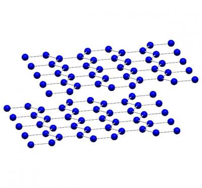 |
| The image shows a bilayer graphene schematic. The blue beads represent carbon atoms.
Credit: Lau lab, UC Riverside |
Abstract:
A research team led by physicists at the University of California, Riverside has identified a property of "bilayer graphene" (BLG) that the researchers say is analogous to finding the Higgs boson in particle physics.
Bilayer graphene works as an insulator: Research by UC Riverside-led team has potential applications in digital and infrared technologies
Riverside, CA | Posted on January 24th, 2012Graphene, nature's thinnest elastic material, is a one-atom thick sheet of carbon atoms arranged in a hexagonal lattice. Because of graphene's planar and chicken wire-like structure, sheets of it lend themselves well to stacking.
BLG is formed when two graphene sheets are stacked in a special manner. Like graphene, BLG has high current-carrying capacity, also known as high electron conductivity. The high current-carrying capacity results from the extremely high velocities that electrons can acquire in a graphene sheet.
The physicists report online Jan. 22 in Nature Nanotechnology that in investigating BLG's properties they found that when the number of electrons on the BLG sheet is close to 0, the material becomes insulating (that is, it resists flow of electrical current) - a finding that has implications for the use of graphene as an electronic material in the semiconductor and electronics industries.
"BLG becomes insulating because its electrons spontaneously organize themselves when their number is small," said Chun Ning (Jeanie) Lau, an associate professor of physics and astronomy and the lead author of the research paper. "Instead of moving around randomly, the electrons move in an orderly fashion. This is called 'spontaneous symmetry breaking' in physics, and is a very important concept since it is the same principle that 'endows' mass for particles in high energy physics."
Lau explained that a typical conductor has a huge number of electrons, which move around randomly, rather like a party with ten thousand guests with no assigned seats at dining tables. If the party only has four guests, however, then the guests will have to interact with each other and sit down at a table. Similarly, when BLG has only a few electrons the interactions cause the electrons to behave in an orderly manner.
New quantum particle
Allan MacDonald, the Sid W. Richardson Foundation Regents Chair in the Department of Physics at The University of Texas at Austin and a coauthor on the research paper, noted that team has measured the mass of a new type of massive quantum particle that can be found only inside BLG crystals.
"The physics which gives these particles their mass is closely analogous to the physics which makes the mass of a proton inside an atomic nucleus very much larger than the mass of the quarks from which it is formed," he said. "Our team's particle is made of electrons, however, not quarks."
MacDonald explained that the experiment the research team conducted was motivated by theoretical work which anticipated that new particles would emerge from the electron sea of a BLG crystal.
"Now that the eagerly anticipated particles have been found, future experiments will help settle an ongoing theoretical debate on their properties," he said.
Practical applications
An important finding of the research team is that the intrinsic "energy gap" in BLG grows with increasing magnetic field.
In solid state physics, an energy gap (or band gap) refers to an energy range in a solid where no electron states can exist. Generally, the size of the energy gap of a material determines whether it is a metal (no gap), semiconductor (small gap) or insulator (large gap). The presence of an energy gap in silicon is critical to the semiconductor industry since, for digital applications, engineers need to turn the device 'on' or conductive, and 'off' or insulating.
Single layer graphene (SLG) is gapless, however, and cannot be completely turned off because regardless of the number of electrons on SLG, it always remains metallic and a conductor.
"This is terribly disadvantageous from an electronics point of view," said Lau, a member of UC Riverside's Center for Nanoscale Science and Engineering. "BLG, on the other hand, can in fact be turned off. Our research is in the initial phase, and, presently, the band gap is still too small for practical applications. What is tremendously exciting though is that this work suggests a promising route - trilayer graphene and tetralayer graphene, which are likely to have much larger energy gaps that can be used for digital and infrared technologies. We already have begun working with these materials."
Lau and MacDonald were joined in the research by J. Velasco Jr. (the first author of the research paper), L. Jing, W. Bao, Y. Lee, P. Kratz, V. Aji, M. Bockrath, and C. Varma at UCR; R. Stillwell and D. Smirnov at the National High Magnetic Field Laboratory, Tallahassee, Fla.; and Fan Zhang and J. Jung at The University of Texas at Austin.
The research was supported by grants from the National Science Foundation, Office of Naval Research, FENA Focus Center, and other agencies.
####
About University of California - Riverside
The University of California, Riverside (www.ucr.edu) is a doctoral research university, a living laboratory for groundbreaking exploration of issues critical to Inland Southern California, the state and communities around the world. Reflecting California's diverse culture, UCR's enrollment has exceeded 20,500 students. The campus will open a medical school in 2013 and has reached the heart of the Coachella Valley by way of the UCR Palm Desert Center. The campus has an annual statewide economic impact of more than $1 billion.
A broadcast studio with fiber cable to the AT&T Hollywood hub is available for live or taped interviews. UCR also has ISDN for radio interviews. To learn more, call 951-UCR-NEWS.
For more information, please click here
Contacts:
Iqbal Pittalwala
951-827-6050
Copyright © University of California - Riverside
If you have a comment, please Contact us.Issuers of news releases, not 7th Wave, Inc. or Nanotechnology Now, are solely responsible for the accuracy of the content.
Bookmark:


| Related News Press |
News and information
![]() Quantum computer improves AI predictions April 17th, 2026
Quantum computer improves AI predictions April 17th, 2026
![]() Flexible sensor gains sensitivity under pressure April 17th, 2026
Flexible sensor gains sensitivity under pressure April 17th, 2026
![]() A reusable chip for particulate matter sensing April 17th, 2026
A reusable chip for particulate matter sensing April 17th, 2026
![]() Detecting vibrational quantum beating in the predissociation dynamics of SF6 using time-resolved photoelectron spectroscopy April 17th, 2026
Detecting vibrational quantum beating in the predissociation dynamics of SF6 using time-resolved photoelectron spectroscopy April 17th, 2026
Physics
![]() UC Irvine physicists discover method to reverse �quantum scrambling� : The work addresses the problem of information loss in quantum computing system April 17th, 2026
UC Irvine physicists discover method to reverse �quantum scrambling� : The work addresses the problem of information loss in quantum computing system April 17th, 2026
![]() Quantum computers simulate fundamental physics: shedding light on the building blocks of nature June 6th, 2025
Quantum computers simulate fundamental physics: shedding light on the building blocks of nature June 6th, 2025
![]() A 1960s idea inspires NBI researchers to study hitherto inaccessible quantum states June 6th, 2025
A 1960s idea inspires NBI researchers to study hitherto inaccessible quantum states June 6th, 2025
![]() Magnetism in new exotic material opens the way for robust quantum computers June 4th, 2025
Magnetism in new exotic material opens the way for robust quantum computers June 4th, 2025
Graphene/ Graphite
![]() Electrifying results shed light on graphene foam as a potential material for lab grown cartilage June 6th, 2025
Electrifying results shed light on graphene foam as a potential material for lab grown cartilage June 6th, 2025
Govt.-Legislation/Regulation/Funding/Policy
![]() Quantum computer improves AI predictions April 17th, 2026
Quantum computer improves AI predictions April 17th, 2026
![]() Metasurfaces smooth light to boost magnetic sensing precision January 30th, 2026
Metasurfaces smooth light to boost magnetic sensing precision January 30th, 2026
![]() New imaging approach transforms study of bacterial biofilms August 8th, 2025
New imaging approach transforms study of bacterial biofilms August 8th, 2025
Chip Technology
![]() A reusable chip for particulate matter sensing April 17th, 2026
A reusable chip for particulate matter sensing April 17th, 2026
![]() Metasurfaces smooth light to boost magnetic sensing precision January 30th, 2026
Metasurfaces smooth light to boost magnetic sensing precision January 30th, 2026
Discoveries
![]() Quantum computer improves AI predictions April 17th, 2026
Quantum computer improves AI predictions April 17th, 2026
![]() Flexible sensor gains sensitivity under pressure April 17th, 2026
Flexible sensor gains sensitivity under pressure April 17th, 2026
![]() A reusable chip for particulate matter sensing April 17th, 2026
A reusable chip for particulate matter sensing April 17th, 2026
![]() Detecting vibrational quantum beating in the predissociation dynamics of SF6 using time-resolved photoelectron spectroscopy April 17th, 2026
Detecting vibrational quantum beating in the predissociation dynamics of SF6 using time-resolved photoelectron spectroscopy April 17th, 2026
Announcements
![]() A fundamentally new therapeutic approach to cystic fibrosis: Nanobody repairs cellular defect April 17th, 2026
A fundamentally new therapeutic approach to cystic fibrosis: Nanobody repairs cellular defect April 17th, 2026
![]() UC Irvine physicists discover method to reverse �quantum scrambling� : The work addresses the problem of information loss in quantum computing system April 17th, 2026
UC Irvine physicists discover method to reverse �quantum scrambling� : The work addresses the problem of information loss in quantum computing system April 17th, 2026
Military
![]() Quantum engineers �squeeze� laser frequency combs to make more sensitive gas sensors January 17th, 2025
Quantum engineers �squeeze� laser frequency combs to make more sensitive gas sensors January 17th, 2025
![]() Chainmail-like material could be the future of armor: First 2D mechanically interlocked polymer exhibits exceptional flexibility and strength January 17th, 2025
Chainmail-like material could be the future of armor: First 2D mechanically interlocked polymer exhibits exceptional flexibility and strength January 17th, 2025
![]() Single atoms show their true color July 5th, 2024
Single atoms show their true color July 5th, 2024
![]() NRL charters Navy�s quantum inertial navigation path to reduce drift April 5th, 2024
NRL charters Navy�s quantum inertial navigation path to reduce drift April 5th, 2024
Research partnerships
![]() Lab to industry: InSe wafer-scale breakthrough for future electronics August 8th, 2025
Lab to industry: InSe wafer-scale breakthrough for future electronics August 8th, 2025
![]() HKU physicists uncover hidden order in the quantum world through deconfined quantum critical points April 25th, 2025
HKU physicists uncover hidden order in the quantum world through deconfined quantum critical points April 25th, 2025
Quantum nanoscience
![]() Beyond silicon: Electronics at the scale of a single molecule January 30th, 2026
Beyond silicon: Electronics at the scale of a single molecule January 30th, 2026
![]() MXene nanomaterials enter a new dimension Multilayer nanomaterial: MXene flakes created at Drexel University show new promise as 1D scrolls January 30th, 2026
MXene nanomaterials enter a new dimension Multilayer nanomaterial: MXene flakes created at Drexel University show new promise as 1D scrolls January 30th, 2026
![]() ICFO researchers overcome long-standing bottleneck in single photon detection with twisted 2D materials August 8th, 2025
ICFO researchers overcome long-standing bottleneck in single photon detection with twisted 2D materials August 8th, 2025
|
|
||
|
|
||
| The latest news from around the world, FREE | ||
|
|
||
|
|
||
| Premium Products | ||
|
|
||
|
Only the news you want to read!
Learn More |
||
|
|
||
|
Full-service, expert consulting
Learn More |
||
|
|
||