Home > Press > Giant Magnetoresistance Emerged from Non-magnetic Phase-change Solid-state Memory - 2000% magnetoresistance ratio at room temperature -
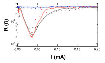 |
| Figure 1 : Switching operation of the PCRAM device
employing the superlattice phase-change film
The magnetoresistance of the device to a magnetic field of 0.1 tesla changes
by 2000% at room temperature. Initial operation with no magnetic field is
shown in red, operation with a magnetic field present is shown in blue,
and operation when the magnetic field is removed is shown in gray. (Copyright: American Institute of Physics) |
Abstract:
- Discovery of a giant magnetic resistance effect at room temperature from a non-magnetic phase-change memory (PCRAM)
- Topological insulating and the Rashba effect emerged from a superlattice phase-change film
- Expected to be applied in ultra-low power consumption next-generation non-volatile memory and logic technologies
Giant Magnetoresistance Emerged from Non-magnetic Phase-change Solid-state Memory - 2000% magnetoresistance ratio at room temperature -
Tokyo, Japan | Posted on January 19th, 2012Junji Tominaga (Prime Senior Researcher) of the Nanoelectronics Research Institute (Director: Seigo Kanemaru) of the National Institute of Advanced Industrial Science and Technology (AIST; President: Tamotsu Nomakuchi) and of Collaborative Research Team Green Nanoelectronics Center (Leader: Naoki Yokoyama), AIST, and others discovered that a superlattice phase-change film multilayered using germanium-tellurium alloy sub-layers and antimony-tellurium alloy sub-layers with aligned orientation axes has a magnetoresistance effect in excess of 2000% in a temperature range from room temperature to around 150 �C. This giant magnetoresistance effect originates in a physical phenomenon known as a topological insulator. It was also discovered that this superlattice phase-change film has a magneto-optical effect in which its optical reflectivity in relation to circularly polarized light in the visible wavelength region (from 400 nm to 800 nm) changes in response to the direction of an external magnetic field.
Thin films of a germanium-antimony-tellurium alloy are typically used in conventional phase-change random access memories (PCRAMs). The research group has engaged in the development of an interfacial phase-change memory multilayered using the germanium-tellurium alloy sub-layers and the antimony-tellurium alloy sub-layers while aligning their orientation axes. The group recently discovered that the memory has a magnetoresistance effect of more than 2000% at room temperature and higher without including any magnetic elements such as cobalt and platinum. The discovery of a room-temperature giant magnetoresistance effect in a PCRAM is expected to lead to an entirely new ultra-high density memory, namely a multiple-functional memory by the fusion or integration of PCRAM and magnetic resistance memory (MRAM) technologies that are being advanced as one of next-generation non-volatile memory technologies. In addition, it is thought that the film has the potential for high-speed switching by an electric field, and it is therefore expected to find application in non-volatile logic technologies.
This research was supported by a grant from the Cabinet Office's Funding Program for World-Leading Innovative R&D on Science and Technology. Details of the results will be published in a scientific journal, "Applied Physics Letters," Vol. 99, No. 15.
Social Background of Research
In the area of next-generation non-volatile memory, attention is being focused on PCRAM, which exploits the difference in electrical resistance between the crystalline and amorphous states of chalcogenide alloys, MRAM, which exploits the difference in electrical resistance generated by a magnetoresistance effect of magnetic alloys, and a resistive random access memory (RRAM), which exploits the difference in electrical resistance generated by the crystalline states of oxides through the application of a strong electric field. PCRAM and MRAM have already been in practical use, but PCRAM has the disadvantage of joule heating to at least the melting point of the memory layer in order to form an amorphous state, significantly increasing power consumption. While, in MRAM, the structural complexity prevents the memory cells from being downsized, and the difference in electrical resistance is significantly smaller than that obtained from PCRAM. In addition, despite the fact that power consumption is relatively lower for RRAM, the principle of its functioning is poorly understood, and it has the fatal disadvantage of limited write-erase cycles.
With the ongoing evolution of mobile IT devices such as smart phones, the radical reduction of the power consumption of solid-state memories and the realization of increased component density and speed are urgent issues, necessitating the development of next-generation non-volatile memories. Competition in the development of solid-state memories, which has been advanced separately, makes management decisions of companies difficult, for example with regard to the development of multiple products and increased manufacturing costs.
History of Research
The "Development of Core Technologies for Green Nanoelectronics" project (Core Researcher: Naoki Yokoyama) of the Cabinet Office's Funding Program for World-Leading Innovative R&D on Science and Technology launched in 2010 as a collaborative R&D project among AIST, private companies, and universities, seeking to reduce the power consumption of next-generation electronic devices. R&D of superlattice phase-change memories has been conducted since then as a subtheme of the research theme "Material Research for Backend Devices" (Theme Leader: Toshimichi Shintani).
Development of PCRAM that operate with low power consumption actually commenced in 2007. In 2004, analysis of the switching mechanism of phase change in germanium-antimony-tellurium alloys used in conventional PCRAM at the atomic level revealed that the valence numbers of germanium atoms are the cause of changes in electrical resistance (AIST press release on September 29, 2004). Since then, the research has been conducted in order to exploit this principle by synthesizing compounds in which change in the valence numbers of germanium atoms is controlled by the atomic displacement with one-dimensionally aligned orientations rather than relying on random three-dimensional transfers, and electrical resistance could be changed without melting. This research has been positioned as one of the core themes of the Funding Program for World-Leading Innovative R&D on Science and Technology since 2010, and the discovery of the giant magnetoresistance effect was made during the course of this research.
Details of Research
The memory layer of the low power consumption PCRAM was a crystalline laminated film formed by multilayering germanium-tellurium and antimony-tellurium crystal sub-layers. The thickness of each crystal sub-layer was determined by quantum mechanics-based simulations known as the first principle simulation. Germanium-tellurium crystals are distorted cubic crystals, while antimony-tellurium crystals have a hexagonal crystal structure. When these two crystal phases are alternately layered, they naturally layer so as to align the c axes (the longitudinal axes) of the hexagonal crystals and the axes connecting the diagonals of the apices of the cubic crystals with an identical direction, which is normal to a substrate surface. Precise control of the thickness of the sub-layers of each alloy based on the simulations enabled a superlattice phase-change film to be formed from different alloys. PCRAM using the superlattice phase-change film was employed in devices, and it was demonstrated that it could be operated using one-tenth or less the power of conventional PCRAM.
The cause of the fact that PCRAM using the superlattice phase-change film has an electrical resistance one order of the magnitude higher than that of PCRAM using the alloy with the same composition, in spite of its high crystallinity, was analyzed. The results showed that the cause was the fact that the antimony-tellurium crystal layers (in a composition ratio of 2:3) possess a special property, topological insulating. Topological insulators have a special pair of cross bands (Draic cones) as part of their electron band structure, enabling electrons to migrate from the valence band to the conduction band without scattering, generating spin current on the surface or the interface. The interesting characteristics of topological insulators are induced by spin-orbit coupling of internal electrons of which velocity is close to light speed, and this effect occurs in materials including heavy elements. In other words, superlattice phase-change films are able to internally generate spin-orbit coupling and an intrinsic magnetic field without including any ferromagnetic element such as cobalt and iron. However, up to the present, physical properties as a topological insulator has only been demonstrated at ultra-low temperatures, and there have been no reported examples emerged at room temperature. However, through first principle simulations, the group found that some of the electron bands in the germanium atoms in germanium-tellurium layers (not a topological insulator) would sprit into the bands with an energy difference of a maximum of 200 meV (the Rashba effect).
Measurement of the change in electrical resistance in a PCRAM employing the superlattice phase-change film in response to a magnetic field at room temperature revealed a giant magnetoresistance effect, with a change in resistance of more than 2000% in response to a 0.1 tesla magnetic field (Fig. 1). In addition, it was confirmed that the voltage required for phase change can be controlled to between 1 and 2 V. The current-voltage characteristic does not obey Ohm's law and stepped changes were confirmed.
A superlattice phase-change film was fabricated on a silicon substrate and differences in the spin-polarized current at the surface of the film due to the Rashba effect were measured. The reflectance of light in the visible wavelength region, from 400 nm to 800 nm, which are far shorter than the band gap energy was measured at room temperature. When a magnetic field was applied, the reflectance of circularly polarized light changed, irrespective of wavelength (Fig. 2). In addition, the reflectance changed even when the magnetic field of different polarization was applied.
This research fabricated the world's first topological insulator functioning at room temperature and higher, in addition to providing the world's first demonstration of the feasibility of spintronics exploiting the Rashba effect, using an artificial superlattice phase-change film. A magnetoresistance effect exceeding 2000 % has never been obtained at room temperature, even when using ferromagnetic materials. The developed superlattice phase-change films are expected to be employed in new devices going beyond memory devices, for example in readout-heads for next-generation hard disk drives.
Future Plans
The replacement of conventional PCRAM recording films with the developed artificial superlattice film will not only reduce power consumption, but will also make it possible to change phase by independently controlling external electrical and magnetic fields, thus enabling control of electrical resistance. PCRAM and MRAM have been considered to be entirely different memory types so far, but the present discovery makes it possible to combine both electrical and magnetic operations in a single memory film, and to produce multiple-valued devices through independent control of parameters, enabling us to expect the future development of ultra-high-density solid-state memories fusing PCRAM and MRAM. Based on the present results, the project will now proceed with research and development of entirely new memory technologies that integrate PCRAM and MRAM.
####
About AIST
The National Institute of Advanced Industrial Science and Technology (AIST), led by President Nomakuchi, is a public research institution funded by the Japanese government to a large extent. The present AIST is a rather new research organization established in 2001. However, AIST and its predecessor organizations have been contributing to society through continuous advancement in technologies and support of Japanese industries since 1882.
Headquarters of AIST are located in Tsukuba and Tokyo. AIST has over 40 autonomous research units in various innovative research fields, and the units are located at nine research bases and several sites (smaller than research bases) of AIST all over Japan. About 2400 researchers (about 2100 with tenure: about 80 from abroad) and thousands of visiting scientists, post-doctoral fellows, and students from home and abroad are working at AIST. About 700 permanent administrative personnel and many temporary staff support research works of AIST.
For more information, please click here
Contacts:
AIST Tokyo Headquarters
1-3-1 Kasumigaseki, Chiyoda-ku, Tokyo 100-8921 Japan
+81-29-861-2000
Copyright © AIST
If you have a comment, please Contact us.Issuers of news releases, not 7th Wave, Inc. or Nanotechnology Now, are solely responsible for the accuracy of the content.
Bookmark:


| Related News Press |
Physics
![]() Simulating magnetization in a Heisenberg quantum spin chain April 5th, 2024
Simulating magnetization in a Heisenberg quantum spin chain April 5th, 2024
News and information
![]() Simulating magnetization in a Heisenberg quantum spin chain April 5th, 2024
Simulating magnetization in a Heisenberg quantum spin chain April 5th, 2024
![]() NRL charters Navy�s quantum inertial navigation path to reduce drift April 5th, 2024
NRL charters Navy�s quantum inertial navigation path to reduce drift April 5th, 2024
![]() Discovery points path to flash-like memory for storing qubits: Rice find could hasten development of nonvolatile quantum memory April 5th, 2024
Discovery points path to flash-like memory for storing qubits: Rice find could hasten development of nonvolatile quantum memory April 5th, 2024
Spintronics
![]() Quantum materials: Electron spin measured for the first time June 9th, 2023
Quantum materials: Electron spin measured for the first time June 9th, 2023
![]() Linearly assembled Ag-Cu nanoclusters: Spin transfer and distance-dependent spin coupling November 4th, 2022
Linearly assembled Ag-Cu nanoclusters: Spin transfer and distance-dependent spin coupling November 4th, 2022
Chip Technology
![]() Discovery points path to flash-like memory for storing qubits: Rice find could hasten development of nonvolatile quantum memory April 5th, 2024
Discovery points path to flash-like memory for storing qubits: Rice find could hasten development of nonvolatile quantum memory April 5th, 2024
![]() Utilizing palladium for addressing contact issues of buried oxide thin film transistors April 5th, 2024
Utilizing palladium for addressing contact issues of buried oxide thin film transistors April 5th, 2024
![]() HKUST researchers develop new integration technique for efficient coupling of III-V and silicon February 16th, 2024
HKUST researchers develop new integration technique for efficient coupling of III-V and silicon February 16th, 2024
Memory Technology
![]() Utilizing palladium for addressing contact issues of buried oxide thin film transistors April 5th, 2024
Utilizing palladium for addressing contact issues of buried oxide thin film transistors April 5th, 2024
![]() Interdisciplinary: Rice team tackles the future of semiconductors Multiferroics could be the key to ultralow-energy computing October 6th, 2023
Interdisciplinary: Rice team tackles the future of semiconductors Multiferroics could be the key to ultralow-energy computing October 6th, 2023
![]() Researchers discover materials exhibiting huge magnetoresistance June 9th, 2023
Researchers discover materials exhibiting huge magnetoresistance June 9th, 2023
Discoveries
![]() Chemical reactions can scramble quantum information as well as black holes April 5th, 2024
Chemical reactions can scramble quantum information as well as black holes April 5th, 2024
![]() New micromaterial releases nanoparticles that selectively destroy cancer cells April 5th, 2024
New micromaterial releases nanoparticles that selectively destroy cancer cells April 5th, 2024
![]() Utilizing palladium for addressing contact issues of buried oxide thin film transistors April 5th, 2024
Utilizing palladium for addressing contact issues of buried oxide thin film transistors April 5th, 2024
Announcements
![]() NRL charters Navy�s quantum inertial navigation path to reduce drift April 5th, 2024
NRL charters Navy�s quantum inertial navigation path to reduce drift April 5th, 2024
![]() Discovery points path to flash-like memory for storing qubits: Rice find could hasten development of nonvolatile quantum memory April 5th, 2024
Discovery points path to flash-like memory for storing qubits: Rice find could hasten development of nonvolatile quantum memory April 5th, 2024
|
|
||
|
|
||
| The latest news from around the world, FREE | ||
|
|
||
|
|
||
| Premium Products | ||
|
|
||
|
Only the news you want to read!
Learn More |
||
|
|
||
|
Full-service, expert consulting
Learn More |
||
|
|
||