Home > Press > Holst Centre and imec launch research program on flexible OLED displays
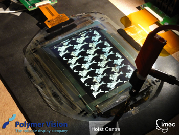 |
| Flexible OLED display developed in close collaboration with Polymer Vision, one of the industrial partners in the shared programs at Holst Centre and imec. |
Abstract:
Holst Centre and imec launch a new research program on next-generation flexible OLED (organic light emitting diode) displays. It builds on their proven technology track record and solid base of existing research partners in related fields such as Organic and Oxide Transistors and Flexible OLED Lighting. The primary objective of the new program is to develop an economically scalable route to high-volume manufacturing of flexible active-matrix OLED displays. The shared program will bring together partners from across the value chain to tackle challenges such as high resolution, low power consumption, large area, outdoor readability, flexibility and light weight.
Holst Centre and imec launch research program on flexible OLED displays
Eindhoven, Netherlands and Leuven, Belgium | Posted on January 17th, 2012Today, state-of-the-art OLED displays are small and mobile and used in applications such as smart phones and tablet PCs. They are characterized by a strong contrast compared to conventional LCDs due to the fact that OLED pixels emit only when activated, achieving a more intense black. Moreover, OLEDs have a faster response time, eliminating image lag. OLEDs can also consume less power, depending on the usage profile, while providing better contrast and viewing angle than conventional LCDs. OLEDs are also much simpler in design and contain less components compared to LCDs, enabling substantial process cost reductions.
The ambition of the new program is work towards flexible, high-resolution OLED displays. The program will tackle the individual challenges towards the next-generation of OLED displays: a mechanically flexible encapsulation film and TFT backplane; and printed, high-efficiency OLEDs. New materials and processes that allow for cheaper production, better quality, lower power, more robustness and more flexibility will be developed. Moreover, the design of the drivers, pixel circuits and TFT backplane matrix will be reconsidered as increasing display area influences the amount of pixels-per-inch or the refresh rates. Finally the program scope includes the development of new manufacturing equipment such as fine patterning equipment for backplanes and tools for integrated roll-to-roll manufacturing.
Gerwin Gelinck (Holst Centre), Program Manager of the OLED Display Program: "Holst Centre and its partners continuously look for new application domains for the generic flexible electronic technologies that have been developed. This ensures our research stays tangible, application-oriented and relevant for industry and society. Flexible displays represent an enormous economic and technical opportunity for flat panel manufacturers and its supply chain. As such they are seen as an attractive landing place for many new technologies. Flexible displays are therefore becoming a top priority research effort for many companies worldwide, including many of our current industrial partners."
Paul Heremans (imec), Program Manager of the OLED Display Program: "With this program in mind, we already have been working more and more towards integrating separate building blocks and have realized OLED displays using both organic and metal oxide TFT backplanes. Thin, plastic substrates were used, and the displays were fully encapsulated using our state-of-the-art barrier technology. Part of this was done with other research institutes in a European project called FLAME, but we could really pull this off because of intense collaboration with some of our industrial partners. We will demonstrate some of these display prototypes in 2012."
####
About IMEC
Imec performs world-leading research in nanoelectronics. Imec leverages its scientific knowledge with the innovative power of its global partnerships in ICT, healthcare and energy. Imec delivers industry-relevant technology solutions. In a unique high-tech environment, its international top talent is committed to providing the building blocks for a better life in a sustainable society. Imec is headquartered in Leuven, Belgium, and has offices in Belgium, the Netherlands, Taiwan, US, China, India and Japan. Its staff of about 1,900 people includes more than 500 industrial residents and guest researchers. In 2010, imec's revenue (P&L) was 285 million euro. Further information on imec can be found at www.imec.be.
Imec is a registered trademark for the activities of IMEC International (a legal entity set up under Belgian law as a "stichting van openbaar nut�), imec Belgium (IMEC vzw supported by the Flemish Government), imec the Netherlands (Stichting IMEC Nederland, part of Holst Centre which is supported by the Dutch Government), imec Taiwan (IMEC Taiwan Co.) and imec China (IMEC Microelectronics (Shangai) Co. Ltd.) and imec India (Imec India Private Limited).
About Holst Centre
Holst Centre is an independent open-innovation R&D centre that develops generic technologies for Wireless Autonomous Sensor Technologies and for Flexible Electronics. A key feature of Holst Centre is its partnership model with industry and academia around shared roadmaps and programs. It is this kind of cross-fertilization that enables Holst Centre to tune its scientific strategy to industrial needs.
Holst Centre was set up in 2005 by imec (Flanders, Belgium) and TNO (The Netherlands) with support from the Dutch Ministry of Economic Affairs and the Government of Flanders. It is named after Gilles Holst, a Dutch pioneer in Research and Development and first director of Philips Research.
Located on High Tech Campus Eindhoven, Holst Centre benefits from the state-of-the-art on-site facilities. Holst Centre has over 170 employees from 28 nationalities and a commitment from over 30 industrial partners. More information: www.holstcentre.com
For more information, please click here
Contacts:
Holst Centre
Koen Snoeckx
Communication Manager
T: +31 (0)40 40 20 561
M: +31 (0)612 71 98 43
Imec
Hanne Degans,
External Communications Officer
T: +32 16 28 17 69
M: +32 486 065 175
Copyright © IMEC
If you have a comment, please Contact us.Issuers of news releases, not 7th Wave, Inc. or Nanotechnology Now, are solely responsible for the accuracy of the content.
Bookmark:


| Related News Press |
News and information
![]() Quantum computer improves AI predictions April 17th, 2026
Quantum computer improves AI predictions April 17th, 2026
![]() Flexible sensor gains sensitivity under pressure April 17th, 2026
Flexible sensor gains sensitivity under pressure April 17th, 2026
![]() A reusable chip for particulate matter sensing April 17th, 2026
A reusable chip for particulate matter sensing April 17th, 2026
![]() Detecting vibrational quantum beating in the predissociation dynamics of SF6 using time-resolved photoelectron spectroscopy April 17th, 2026
Detecting vibrational quantum beating in the predissociation dynamics of SF6 using time-resolved photoelectron spectroscopy April 17th, 2026
Display technology/LEDs/SS Lighting/OLEDs
![]() Spinel-type sulfide semiconductors to operate the next-generation LEDs and solar cells For solar-cell absorbers and green-LED source October 3rd, 2025
Spinel-type sulfide semiconductors to operate the next-generation LEDs and solar cells For solar-cell absorbers and green-LED source October 3rd, 2025
![]() Efficient and stable hybrid perovskite-organic light-emitting diodes with external quantum efficiency exceeding 40 per cent July 5th, 2024
Efficient and stable hybrid perovskite-organic light-emitting diodes with external quantum efficiency exceeding 40 per cent July 5th, 2024
Announcements
![]() A fundamentally new therapeutic approach to cystic fibrosis: Nanobody repairs cellular defect April 17th, 2026
A fundamentally new therapeutic approach to cystic fibrosis: Nanobody repairs cellular defect April 17th, 2026
![]() UC Irvine physicists discover method to reverse �quantum scrambling� : The work addresses the problem of information loss in quantum computing system April 17th, 2026
UC Irvine physicists discover method to reverse �quantum scrambling� : The work addresses the problem of information loss in quantum computing system April 17th, 2026
Alliances/Trade associations/Partnerships/Distributorships
![]() Chicago Quantum Exchange welcomes six new partners highlighting quantum technology solutions, from Chicago and beyond September 23rd, 2022
Chicago Quantum Exchange welcomes six new partners highlighting quantum technology solutions, from Chicago and beyond September 23rd, 2022
![]() University of Illinois Chicago joins Brookhaven Lab's Quantum Center June 10th, 2022
University of Illinois Chicago joins Brookhaven Lab's Quantum Center June 10th, 2022
Research partnerships
![]() Lab to industry: InSe wafer-scale breakthrough for future electronics August 8th, 2025
Lab to industry: InSe wafer-scale breakthrough for future electronics August 8th, 2025
![]() HKU physicists uncover hidden order in the quantum world through deconfined quantum critical points April 25th, 2025
HKU physicists uncover hidden order in the quantum world through deconfined quantum critical points April 25th, 2025
|
|
||
|
|
||
| The latest news from around the world, FREE | ||
|
|
||
|
|
||
| Premium Products | ||
|
|
||
|
Only the news you want to read!
Learn More |
||
|
|
||
|
Full-service, expert consulting
Learn More |
||
|
|
||