Home > Press > ORNL experiments prove nanoscale metallic conductivity in ferroelectrics
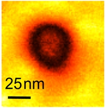 |
| ORNL researchers used piezoresponse force microscopy to demonstrate the first evidence of metallic conductivity in ferroelectric nanodomains. A representative nanodomain is shown in the PFM image above. |
Abstract:
The prospect of electronics at the nanoscale may be even more promising with the first observation of metallic conductance in ferroelectric nanodomains by researchers at Oak Ridge National Laboratory.
ORNL experiments prove nanoscale metallic conductivity in ferroelectrics
Oak Ridge, TN | Posted on January 9th, 2012Ferroelectric materials, which switch their polarization with the application of an electric field, have long been used in devices such as ultrasound machines and sensors. Now, discoveries about ferroelectrics' electronic properties are opening up possibilities of applications in nanoscale electronics and information storage.
In a paper published in the American Chemical Society's Nano Letters, the ORNL-led team demonstrated metallic conductivity in a ferroelectric film that otherwise acts as an insulator. This phenomenon of an insulator-metal transition was predicted more than 40 years ago by theorists but has eluded experimental proof until now.
"This finding unambiguously identifies a new conduction channel that percolates through the insulating matrix of the ferroelectric, which opens potentially exciting possibilities to 'write' and 'erase' circuitry with nanoscale dimensions," said lead author Peter Maksymovych of ORNL's Center for Nanophase Materials Sciences.
From an applied perspective, the ability to use only an electric field as a knob that tunes both the magnitude of metallic conductivity in a ferroelectric and the type of charge carriers is particularly intriguing. Doing the latter in a semiconductor would require a change of the material composition.
"Not only can we turn on metallic conductivity, but if you keep changing the bias dials, you can control the behavior very precisely," Maksymovych said. "And the smaller the nanodomain, the better it conducts. All this occurs in the exact same position of the material, and we can go from an insulator to a better metal or a worse metal in a heartbeat or faster. This is potentially attractive for applications, and it also leads to interesting fundamental questions about the exact mechanism of metallic conductivity."
Although the researchers focused their study on a well-known ferroelectric film called lead-zirconate titanate, they expect their observations will hold true for a broader array of ferroelectric materials.
"We also anticipate that extending our studies onto multiferroics, mixed-phase and anti-ferroelectrics will reveal a whole family of previously unknown electronic properties, breaking new ground in fundamentals and applications alike," said co-author and ORNL senior scientist Sergei Kalinin.
The samples used in the study were provided by the University of California at Berkeley. Co-authors on the paper are ORNL's Arthur Baddorf, UC Berkeley's Ying-Hao Chu, Ramamoorthy Ramesh and Pu Yu, and National Academy of Science of Ukraine's Eugene Eliseev and Anna Morozovska. The full paper, "Tunable Metallic Conductance in Ferroelectric Nanodomains," is available at pubs.acs.org/doi/full/10.1021/nl203349b.
Part of this work was supported by the Center for Nanophase Materials Sciences at ORNL. CNMS is one of the five DOE Nanoscale Science Research Centers supported by the DOE Office of Science, premier national user facilities for interdisciplinary research at the nanoscale. Together the NSRCs comprise a suite of complementary facilities that provide researchers with state-of-the-art capabilities to fabricate, process, characterize and model nanoscale materials, and constitute the largest infrastructure investment of the National Nanotechnology Initiative. The NSRCs are located at DOE's Argonne, Brookhaven, Lawrence Berkeley, Oak Ridge and Sandia and Los Alamos national laboratories. For more information about the DOE NSRCs, please visit science.energy.gov/bes/suf/user-facilities/nanoscale-science-research-centers/. Work at the University of California, Berkeley, was supported by DOE's Office of Science and the Semiconductor Research Corporation. ORNL is managed by UT-Battelle for the Department of Energy's Office of Science.
####
For more information, please click here
Contacts:
Morgan McCorkle
Communications and Media Relations
865.574.7308
Copyright © Oak Ridge National Laboratory
If you have a comment, please Contact us.Issuers of news releases, not 7th Wave, Inc. or Nanotechnology Now, are solely responsible for the accuracy of the content.
Bookmark:


| Related News Press |
Physics
![]() Simulating magnetization in a Heisenberg quantum spin chain April 5th, 2024
Simulating magnetization in a Heisenberg quantum spin chain April 5th, 2024
![]() 'Sudden death' of quantum fluctuations defies current theories of superconductivity: Study challenges the conventional wisdom of superconducting quantum transitions January 12th, 2024
'Sudden death' of quantum fluctuations defies current theories of superconductivity: Study challenges the conventional wisdom of superconducting quantum transitions January 12th, 2024
News and information
![]() Simulating magnetization in a Heisenberg quantum spin chain April 5th, 2024
Simulating magnetization in a Heisenberg quantum spin chain April 5th, 2024
![]() NRL charters Navy�s quantum inertial navigation path to reduce drift April 5th, 2024
NRL charters Navy�s quantum inertial navigation path to reduce drift April 5th, 2024
![]() Discovery points path to flash-like memory for storing qubits: Rice find could hasten development of nonvolatile quantum memory April 5th, 2024
Discovery points path to flash-like memory for storing qubits: Rice find could hasten development of nonvolatile quantum memory April 5th, 2024
Laboratories
![]() A battery�s hopping ions remember where they�ve been: Seen in atomic detail, the seemingly smooth flow of ions through a battery�s electrolyte is surprisingly complicated February 16th, 2024
A battery�s hopping ions remember where they�ve been: Seen in atomic detail, the seemingly smooth flow of ions through a battery�s electrolyte is surprisingly complicated February 16th, 2024
![]() NRL discovers two-dimensional waveguides February 16th, 2024
NRL discovers two-dimensional waveguides February 16th, 2024
Insurance
![]() Multi-million pound project to use nanotechnology to improve safety September 4th, 2015
Multi-million pound project to use nanotechnology to improve safety September 4th, 2015
![]() Research seeks alternatives for reducing bacteria in fresh produce using nanoengineering April 29th, 2015
Research seeks alternatives for reducing bacteria in fresh produce using nanoengineering April 29th, 2015
![]() Liquipel Adds Guarantee to Watersafe Nano-Coating Products at CES: Announced at Booth 25936, South Hall; Billions in Hardware Damage to Be Saved January 8th, 2013
Liquipel Adds Guarantee to Watersafe Nano-Coating Products at CES: Announced at Booth 25936, South Hall; Billions in Hardware Damage to Be Saved January 8th, 2013
![]() Emerging Risks Report: Examining the case for Insurance in Engineered Nanomaterials December 29th, 2010
Emerging Risks Report: Examining the case for Insurance in Engineered Nanomaterials December 29th, 2010
Govt.-Legislation/Regulation/Funding/Policy
![]() NRL charters Navy�s quantum inertial navigation path to reduce drift April 5th, 2024
NRL charters Navy�s quantum inertial navigation path to reduce drift April 5th, 2024
![]() Discovery points path to flash-like memory for storing qubits: Rice find could hasten development of nonvolatile quantum memory April 5th, 2024
Discovery points path to flash-like memory for storing qubits: Rice find could hasten development of nonvolatile quantum memory April 5th, 2024
![]() Chemical reactions can scramble quantum information as well as black holes April 5th, 2024
Chemical reactions can scramble quantum information as well as black holes April 5th, 2024
Chip Technology
![]() Discovery points path to flash-like memory for storing qubits: Rice find could hasten development of nonvolatile quantum memory April 5th, 2024
Discovery points path to flash-like memory for storing qubits: Rice find could hasten development of nonvolatile quantum memory April 5th, 2024
![]() Utilizing palladium for addressing contact issues of buried oxide thin film transistors April 5th, 2024
Utilizing palladium for addressing contact issues of buried oxide thin film transistors April 5th, 2024
![]() HKUST researchers develop new integration technique for efficient coupling of III-V and silicon February 16th, 2024
HKUST researchers develop new integration technique for efficient coupling of III-V and silicon February 16th, 2024
Discoveries
![]() Chemical reactions can scramble quantum information as well as black holes April 5th, 2024
Chemical reactions can scramble quantum information as well as black holes April 5th, 2024
![]() New micromaterial releases nanoparticles that selectively destroy cancer cells April 5th, 2024
New micromaterial releases nanoparticles that selectively destroy cancer cells April 5th, 2024
![]() Utilizing palladium for addressing contact issues of buried oxide thin film transistors April 5th, 2024
Utilizing palladium for addressing contact issues of buried oxide thin film transistors April 5th, 2024
Announcements
![]() NRL charters Navy�s quantum inertial navigation path to reduce drift April 5th, 2024
NRL charters Navy�s quantum inertial navigation path to reduce drift April 5th, 2024
![]() Discovery points path to flash-like memory for storing qubits: Rice find could hasten development of nonvolatile quantum memory April 5th, 2024
Discovery points path to flash-like memory for storing qubits: Rice find could hasten development of nonvolatile quantum memory April 5th, 2024
|
|
||
|
|
||
| The latest news from around the world, FREE | ||
|
|
||
|
|
||
| Premium Products | ||
|
|
||
|
Only the news you want to read!
Learn More |
||
|
|
||
|
Full-service, expert consulting
Learn More |
||
|
|
||