Home > Press > Researchers measure nanometer scale temperature: Nanometer scale temperature
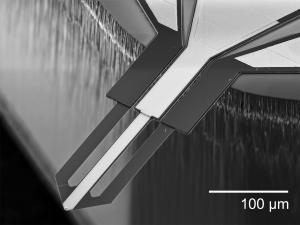 |
| This is an electrothermal cantilever from the University of Illinois, having nanometer-scale electrode tip integrated onto a microheater.
Credit: University of Illinois at Urbana-Champaign |
Abstract:
Atomic force microscope cantilever tips with integrated heaters are widely used to characterize polymer films in electronics and optical devices, pharmaceuticals, paints, and coatings. These heated tips are also used in research labs to explore new ideas in nanolithography and data storage, and to study fundamentals of nanometer-scale heat flow. Until now, however, no one has used a heated nano-tip for electronic measurements.
Researchers measure nanometer scale temperature: Nanometer scale temperature
Urbana, IL | Posted on December 19th, 2011"We have developed a new kind of electro-thermal nanoprobe," according to William King, a College of Engineering Bliss Professor in the Department of Mechanical Science and Engineering at the University of Illinois at Urbana-Champaign. "Our electro-thermal nanoprobe can independently control voltage and temperature at a nanometer-scale point contact. It can also measure the temperature-dependent voltage at a nanometer-scale point contact."
"Our goal is to perform electro-thermal measurements at the nanometer scale," according to Patrick Fletcher, first author of the paper, "Thermoelectric voltage at a nanometer-scale heated tip point contact," published in the journal Nanotechnology. "Our electro-thermal nanoprobe can be used to measure the nanometer-scale properties of materials such as semiconductors, thermoelectrics, and ferroelectrics."
The electro-thermal probes are different than thermal nanoprobes typically used in King's group and elsewhere. They have three electrical paths to the cantilever tip. Two of the paths carry heating current, while the third allows the nanometer-scale electrical measurement. The two electrical paths are separated by a diode junction fabricated into the tip. While the cantilever design is complex, the probes can be used in any atomic force microscope.
In addition to Fletcher, co-authors of the paper include Byeonghee Lee, and William King. The research was performed in the Nanoengineering laboratory as well as the Micro and Nanotechnology Laboratory and the Materials Research Laboratory at the University of Illinois.
The paper is available online at doi:10.1088/0957-4484/23/3/035401
The research was sponsored by the Office of Naval Research and the Air Force Office of Scientific Research.
####
For more information, please click here
Contacts:
William King
217-244-3864
Copyright © University of Illinois College of Engineering
If you have a comment, please Contact us.Issuers of news releases, not 7th Wave, Inc. or Nanotechnology Now, are solely responsible for the accuracy of the content.
Bookmark:


| Related News Press |
News and information
![]() Quantum computer improves AI predictions April 17th, 2026
Quantum computer improves AI predictions April 17th, 2026
![]() Flexible sensor gains sensitivity under pressure April 17th, 2026
Flexible sensor gains sensitivity under pressure April 17th, 2026
![]() A reusable chip for particulate matter sensing April 17th, 2026
A reusable chip for particulate matter sensing April 17th, 2026
![]() Detecting vibrational quantum beating in the predissociation dynamics of SF6 using time-resolved photoelectron spectroscopy April 17th, 2026
Detecting vibrational quantum beating in the predissociation dynamics of SF6 using time-resolved photoelectron spectroscopy April 17th, 2026
Govt.-Legislation/Regulation/Funding/Policy
![]() Quantum computer improves AI predictions April 17th, 2026
Quantum computer improves AI predictions April 17th, 2026
![]() Metasurfaces smooth light to boost magnetic sensing precision January 30th, 2026
Metasurfaces smooth light to boost magnetic sensing precision January 30th, 2026
![]() New imaging approach transforms study of bacterial biofilms August 8th, 2025
New imaging approach transforms study of bacterial biofilms August 8th, 2025
Discoveries
![]() Quantum computer improves AI predictions April 17th, 2026
Quantum computer improves AI predictions April 17th, 2026
![]() Flexible sensor gains sensitivity under pressure April 17th, 2026
Flexible sensor gains sensitivity under pressure April 17th, 2026
![]() A reusable chip for particulate matter sensing April 17th, 2026
A reusable chip for particulate matter sensing April 17th, 2026
![]() Detecting vibrational quantum beating in the predissociation dynamics of SF6 using time-resolved photoelectron spectroscopy April 17th, 2026
Detecting vibrational quantum beating in the predissociation dynamics of SF6 using time-resolved photoelectron spectroscopy April 17th, 2026
Announcements
![]() A fundamentally new therapeutic approach to cystic fibrosis: Nanobody repairs cellular defect April 17th, 2026
A fundamentally new therapeutic approach to cystic fibrosis: Nanobody repairs cellular defect April 17th, 2026
![]() UC Irvine physicists discover method to reverse �quantum scrambling� : The work addresses the problem of information loss in quantum computing system April 17th, 2026
UC Irvine physicists discover method to reverse �quantum scrambling� : The work addresses the problem of information loss in quantum computing system April 17th, 2026
Tools
![]() Metasurfaces smooth light to boost magnetic sensing precision January 30th, 2026
Metasurfaces smooth light to boost magnetic sensing precision January 30th, 2026
![]() From sensors to smart systems: the rise of AI-driven photonic noses January 30th, 2026
From sensors to smart systems: the rise of AI-driven photonic noses January 30th, 2026
![]() Japan launches fully domestically produced quantum computer: Expo visitors to experience quantum computing firsthand August 8th, 2025
Japan launches fully domestically produced quantum computer: Expo visitors to experience quantum computing firsthand August 8th, 2025
Military
![]() Quantum engineers �squeeze� laser frequency combs to make more sensitive gas sensors January 17th, 2025
Quantum engineers �squeeze� laser frequency combs to make more sensitive gas sensors January 17th, 2025
![]() Chainmail-like material could be the future of armor: First 2D mechanically interlocked polymer exhibits exceptional flexibility and strength January 17th, 2025
Chainmail-like material could be the future of armor: First 2D mechanically interlocked polymer exhibits exceptional flexibility and strength January 17th, 2025
![]() Single atoms show their true color July 5th, 2024
Single atoms show their true color July 5th, 2024
![]() NRL charters Navy�s quantum inertial navigation path to reduce drift April 5th, 2024
NRL charters Navy�s quantum inertial navigation path to reduce drift April 5th, 2024
|
|
||
|
|
||
| The latest news from around the world, FREE | ||
|
|
||
|
|
||
| Premium Products | ||
|
|
||
|
Only the news you want to read!
Learn More |
||
|
|
||
|
Full-service, expert consulting
Learn More |
||
|
|
||