Home > Press > New method of growing high-quality graphene promising for next-gen technology: Method refined by UC Santa Barbara scientists to synthesize sheets of 'wonder material' graphene is promising link to futuristic technology
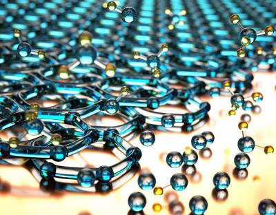 |
| UCSB researchers have successfully controlled the growth of a high-quality bilayer graphene on a copper substrate using a method called chemical vapor deposition (CVD), which breaks down molecules of methane gas to build graphene sheets with carbon atoms.
Credit: Peter Allen |
Abstract:
Making waves as the material that will revolutionize electronics, graphene - composed of a single layer of Carbon atoms - has nonetheless been challenging to produce in a way that will be practical for innovative electronics applications. Researchers at UC Santa Barbara have discovered a method to synthesize high quality graphene in a controlled manner that may pave the way for next-generation electronics application.
New method of growing high-quality graphene promising for next-gen technology: Method refined by UC Santa Barbara scientists to synthesize sheets of 'wonder material' graphene is promising link to futuristic technology
Santa Barbara, CA | Posted on October 17th, 2011Kaustav Banerjee, a professor with the Electrical and Computer Engineering department and Director of the Nanoelectronics Research Lab at UCSB that has been studying carbon nanomaterials for more than seven years, led the research team to perfect methods of growing sheets of graphene, as detailed in a study to be published in the November 2011 issue of the journal Carbon.
"Our process has certain unique advantages that give rise to high quality graphene," says Banerjee. "For the electronics industry to effectively use graphene, it must first be grown selectively and in larger sheets. We have developed a synthesis technique that yields high- quality and high-uniformity graphene that can be translated into a scalable process for industry applications."
Using adhesive tape to lift flakes of graphene from graphite, University of Manchester researchers Geim and Novoselov were awarded the 2010 Nobel Prize in Physics for their pioneering isolation and characterization of the material. To launch graphene into futuristic applications, however, researchers have been seeking a controlled and efficient way to grow a higher quality of this single-atom-thick material in larger areas.
The discovery by UCSB researchers turns graphene production into an industry-friendly process by improving the quality and uniformity of graphene using efficient and reproducible methods. They were able to control the number of graphene layers produced - from mono-layer to bi-layer graphene - an important distinction for future applications in electronics and other technology.
"Intel has a keen interest in graphene due to many possibilities it holds for the next generation of energy- efficient computing, but there are many roadblocks along the way," added Intel Fellow, Shekhar Borkar. "The scalable synthesis technique developed by Professor Banerjee's group at UCSB is an important step forward."
As a material, graphene is the thinnest and strongest in the world - more than 100 times stronger than diamond - and is capable of acting as an ultimate conductor at room temperature. If it can be produced effectively, graphene's properties make it ideal for advancements in green electronics, super strong materials, and medical technology. Graphene could be used to make flexible screens and electronic devices, computers with 1,000 GHz processors that run on virtually no energy, and ultra-efficient solar power cells.
Key to the UCSB team's discovery is their understanding of graphene growth kinetics under the influence of the substrate. Their approach uses a method called low pressure chemical vapor deposition (LPCVD) and involves disintegrating the hydrocarbon gas methane at a specific high temperature to build uniform layers of carbon (as graphene) on a pretreated copper substrate. Banerjee's research group established a set of techniques that optimized the uniformity and quality of graphene, while controlling the number of graphene layers they grew on their substrate.
According to Dr. Wei Liu, a post-doctoral researcher and co-author of the study, "Graphene growth is strongly affected by imperfection sites on the copper substrate. By proper treatment of the copper surface and precise selection of the growth parameters, the quality and uniformity of graphene are significantly improved and the number of graphene layers can be controlled."
Professor Banerjee and credited authors Wei Liu, Hong Li, Chuan Xu and Yasin Khatami are not the first research team to make graphene using the CVD method, but they are the first to successfully refine critical methods to grow a high quality of graphene. In the past, a key challenge for the CVD method has been that it yields a lower quality of graphene in terms of carrier mobility - or how well it conducts electrons. "Our graphene exhibits the highest reported field-effect mobility to date for CVD graphene, having an average value of 4000 cm2/V.s with the highest peak value at 5500 cm2/V.s. This is an extremely high value compared with the mobility of silicon." added Hong Li, a Ph.D. candidate in Banerjee's research group.
"Kaustav Banerjee's group is leading graphene nanoelectronics research efforts at UCSB, from material synthesis to device design and circuit exploration. His work has provided our campus with unique and very powerful capabilities," added David Awschalom, Professor of Physics, Electrical and Computer Engineering, and Director of the California NanoSystems Institute (CNSI) at UCSB where Banerjee's laboratory is located. "This new facility has also boosted our opportunities for collaborations across various science and engineering disciplines."
"There is no doubt graphene is a superior material. Intrinsically it is amazing," says Banerjee. "It is up to us, the scientists and engineers, to show how we can use graphene and harness its capabilities. There are challenges in how to grow it, how to transfer or not to transfer and pattern it, and how to tailor its properties for specific applications. But these challenges are fertile grounds for exciting research in the future."
Their research was supported by the National Science Foundation and conducted at the California NanoSystems Institute (CNSI) and Materials Research Laboratory (MRL) facilities at UC Santa Barbara.
####
For more information, please click here
Contacts:
Melissa Van De Werfhorst
805-893-4301
Copyright © University of California - Santa Barbara
If you have a comment, please Contact us.Issuers of news releases, not 7th Wave, Inc. or Nanotechnology Now, are solely responsible for the accuracy of the content.
Bookmark:


| Related News Press |
News and information
![]() Quantum computer improves AI predictions April 17th, 2026
Quantum computer improves AI predictions April 17th, 2026
![]() Flexible sensor gains sensitivity under pressure April 17th, 2026
Flexible sensor gains sensitivity under pressure April 17th, 2026
![]() A reusable chip for particulate matter sensing April 17th, 2026
A reusable chip for particulate matter sensing April 17th, 2026
![]() Detecting vibrational quantum beating in the predissociation dynamics of SF6 using time-resolved photoelectron spectroscopy April 17th, 2026
Detecting vibrational quantum beating in the predissociation dynamics of SF6 using time-resolved photoelectron spectroscopy April 17th, 2026
Graphene/ Graphite
![]() Electrifying results shed light on graphene foam as a potential material for lab grown cartilage June 6th, 2025
Electrifying results shed light on graphene foam as a potential material for lab grown cartilage June 6th, 2025
![]() Breakthrough in proton barrier films using pore-free graphene oxide: Kumamoto University researchers achieve new milestone in advanced coating technologies September 13th, 2024
Breakthrough in proton barrier films using pore-free graphene oxide: Kumamoto University researchers achieve new milestone in advanced coating technologies September 13th, 2024
Govt.-Legislation/Regulation/Funding/Policy
![]() Quantum computer improves AI predictions April 17th, 2026
Quantum computer improves AI predictions April 17th, 2026
![]() Metasurfaces smooth light to boost magnetic sensing precision January 30th, 2026
Metasurfaces smooth light to boost magnetic sensing precision January 30th, 2026
![]() New imaging approach transforms study of bacterial biofilms August 8th, 2025
New imaging approach transforms study of bacterial biofilms August 8th, 2025
Chip Technology
![]() A reusable chip for particulate matter sensing April 17th, 2026
A reusable chip for particulate matter sensing April 17th, 2026
![]() Metasurfaces smooth light to boost magnetic sensing precision January 30th, 2026
Metasurfaces smooth light to boost magnetic sensing precision January 30th, 2026
Discoveries
![]() Quantum computer improves AI predictions April 17th, 2026
Quantum computer improves AI predictions April 17th, 2026
![]() Flexible sensor gains sensitivity under pressure April 17th, 2026
Flexible sensor gains sensitivity under pressure April 17th, 2026
![]() A reusable chip for particulate matter sensing April 17th, 2026
A reusable chip for particulate matter sensing April 17th, 2026
![]() Detecting vibrational quantum beating in the predissociation dynamics of SF6 using time-resolved photoelectron spectroscopy April 17th, 2026
Detecting vibrational quantum beating in the predissociation dynamics of SF6 using time-resolved photoelectron spectroscopy April 17th, 2026
Announcements
![]() A fundamentally new therapeutic approach to cystic fibrosis: Nanobody repairs cellular defect April 17th, 2026
A fundamentally new therapeutic approach to cystic fibrosis: Nanobody repairs cellular defect April 17th, 2026
![]() UC Irvine physicists discover method to reverse �quantum scrambling� : The work addresses the problem of information loss in quantum computing system April 17th, 2026
UC Irvine physicists discover method to reverse �quantum scrambling� : The work addresses the problem of information loss in quantum computing system April 17th, 2026
Energy
![]() Sensors innovations for smart lithium-based batteries: advancements, opportunities, and potential challenges August 8th, 2025
Sensors innovations for smart lithium-based batteries: advancements, opportunities, and potential challenges August 8th, 2025
![]() Simple algorithm paired with standard imaging tool could predict failure in lithium metal batteries August 8th, 2025
Simple algorithm paired with standard imaging tool could predict failure in lithium metal batteries August 8th, 2025
Solar/Photovoltaic
![]() Spinel-type sulfide semiconductors to operate the next-generation LEDs and solar cells For solar-cell absorbers and green-LED source October 3rd, 2025
Spinel-type sulfide semiconductors to operate the next-generation LEDs and solar cells For solar-cell absorbers and green-LED source October 3rd, 2025
![]() KAIST researchers introduce new and improved, next-generation perovskite solar cell November 8th, 2024
KAIST researchers introduce new and improved, next-generation perovskite solar cell November 8th, 2024
![]() Groundbreaking precision in single-molecule optoelectronics August 16th, 2024
Groundbreaking precision in single-molecule optoelectronics August 16th, 2024
![]() Development of zinc oxide nanopagoda array photoelectrode: photoelectrochemical water-splitting hydrogen production January 12th, 2024
Development of zinc oxide nanopagoda array photoelectrode: photoelectrochemical water-splitting hydrogen production January 12th, 2024
|
|
||
|
|
||
| The latest news from around the world, FREE | ||
|
|
||
|
|
||
| Premium Products | ||
|
|
||
|
Only the news you want to read!
Learn More |
||
|
|
||
|
Full-service, expert consulting
Learn More |
||
|
|
||