Home > Press > Imec demonstrates CMOS integrated poly-SiGe piezoresistive pressure sensor
 |
Abstract:
Imec realized an integrated poly-SiGe-based piezoresistive pressure sensor directly fabricated above 0.13 µm copper (Cu) -backend CMOS technology. This represents not only the first integrated poly-SiGe pressure sensor directly fabricated above its readout circuit, but also the first time that a poly-SiGe MEMS device is processed on top of Cu-backend CMOS.
Imec demonstrates CMOS integrated poly-SiGe piezoresistive pressure sensor
Leuven, Belgium | Posted on October 10th, 2011Polycrystalline SiGe has emerged as a promising MEMS structural material since it provides the desired mechanical properties at lower temperatures compared to poly-Si, allowing the post-processing on top of CMOS. The MEMS-last approach is the most interesting approach for CMOS-MEMS monolithic integration as it leads to smaller die areas and enables integrating the MEMS without introducing any changes in standard foundry CMOS processes. Comparing to alternative technologies, for example using the CMOS top interconnect layers to fabricate the MEMS device, poly-SiGe offers a more generic and flexible technology for above CMOS integration, thanks to the fact that the MEMS fabrication can be completely decoupled from the CMOS fabrication.
In the past, imec already proved the potential of poly-SiGe for MEMS above-aluminum-backend CMOS integration. However, aggressive interconnect scaling has led to the replacement of the traditional aluminum metallization by copper metallization, due to its lower resistivity and improved reliability. Our results now broaden the applications of poly-SiGe to the integration of MEMS with the advanced CMOS technology nodes.
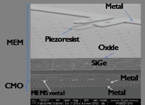
Our integrated sensor (fully fabricated in imec) includes a surface-micromachined piezoresistive pressure sensor, with a poly-SiGe membrane and four poly-SiGe piezoresistors, and an instrumentation amplifier fabricated using imec's 0.13 m standard CMOS technology, with Cu- interconnects (two metal layers), oxide dielectric and tungsten-filled vias. To enable above-CMOS integration the maximum processing temperature of the complete sensor, including the poly-SiGe piezoresistors, is kept below 455şC. Moreover, an appropriate passivation layer was included to protect the electronic circuit from the aggressive etch and deposition steps needed to fabricate the MEMS devices. The CMOS circuit showed no significant deterioration after the MEMS processing. Despite the low processing temperature, the poly-SiGe piezoresistive sensor alone (250x250µm2 membrane) showed a sensitivity of around 2.5 mV/V/bar. The integrated sensor (same sensor + Cu-based CMOS amplifier underneath) showed a sensitivity of about 158 mV/V/bar, ~64 times higher than the stand-alone sensor.
####
About IMEC
Imec performs world-leading research in nanoelectronics. Imec leverages its scientific knowledge with the innovative power of its global partnerships in ICT, healthcare and energy. Imec delivers industry-relevant technology solutions. In a unique high-tech environment, its international top talent is committed to providing the building blocks for a better life in a sustainable society. Imec is headquartered in Leuven, Belgium, and has offices in Belgium, the Netherlands, Taiwan, US, China, India and Japan. Its staff of about 1,900 people includes more than 500 industrial residents and guest researchers. In 2010, imec's revenue (P&L) was 285 million euro. Further information on imec can be found at www.imec.be.
Imec is a registered trademark for the activities of IMEC International (a legal entity set up under Belgian law as a "stichting van openbaar nut”), imec Belgium (IMEC vzw supported by the Flemish Government), imec the Netherlands (Stichting IMEC Nederland, part of Holst Centre which is supported by the Dutch Government), imec Taiwan (IMEC Taiwan Co.) and imec China (IMEC Microelectronics (Shangai) Co. Ltd.) and imec India (Imec India Private Limited).
For more information, please click here
Contacts:
Hanne Degans
External Communications Officer
T: +32 16 28 17 69
M: +32 486 065 175
Barbara Kalkis
Maestro Marketing & PR
T: +1 408 996 9975
Copyright © IMEC
If you have a comment, please Contact us.Issuers of news releases, not 7th Wave, Inc. or Nanotechnology Now, are solely responsible for the accuracy of the content.
Bookmark:


| Related News Press |
News and information
![]() Simulating magnetization in a Heisenberg quantum spin chain April 5th, 2024
Simulating magnetization in a Heisenberg quantum spin chain April 5th, 2024
![]() NRL charters Navy’s quantum inertial navigation path to reduce drift April 5th, 2024
NRL charters Navy’s quantum inertial navigation path to reduce drift April 5th, 2024
![]() Discovery points path to flash-like memory for storing qubits: Rice find could hasten development of nonvolatile quantum memory April 5th, 2024
Discovery points path to flash-like memory for storing qubits: Rice find could hasten development of nonvolatile quantum memory April 5th, 2024
Chip Technology
![]() Discovery points path to flash-like memory for storing qubits: Rice find could hasten development of nonvolatile quantum memory April 5th, 2024
Discovery points path to flash-like memory for storing qubits: Rice find could hasten development of nonvolatile quantum memory April 5th, 2024
![]() Utilizing palladium for addressing contact issues of buried oxide thin film transistors April 5th, 2024
Utilizing palladium for addressing contact issues of buried oxide thin film transistors April 5th, 2024
![]() HKUST researchers develop new integration technique for efficient coupling of III-V and silicon February 16th, 2024
HKUST researchers develop new integration technique for efficient coupling of III-V and silicon February 16th, 2024
Sensors
Announcements
![]() NRL charters Navy’s quantum inertial navigation path to reduce drift April 5th, 2024
NRL charters Navy’s quantum inertial navigation path to reduce drift April 5th, 2024
![]() Discovery points path to flash-like memory for storing qubits: Rice find could hasten development of nonvolatile quantum memory April 5th, 2024
Discovery points path to flash-like memory for storing qubits: Rice find could hasten development of nonvolatile quantum memory April 5th, 2024
|
|
||
|
|
||
| The latest news from around the world, FREE | ||
|
|
||
|
|
||
| Premium Products | ||
|
|
||
|
Only the news you want to read!
Learn More |
||
|
|
||
|
Full-service, expert consulting
Learn More |
||
|
|
||